Method for eliminating surface defect of semiconductor device and semiconductor device

A device surface, semiconductor technology, used in semiconductor/solid-state device manufacturing, electrical components, circuits, etc., can solve problems affecting wiring integrity, epitaxy front lines, pattern defects, etc., to eliminate surface defects, reduce pollution, and improve yield. Effect

Active Publication Date: 2010-06-16
SEMICON MFG INT (SHANGHAI) CORP
View PDF0 Cites 12 Cited by
  • Summary
  • Abstract
  • Description
  • Claims
  • Application Information

AI Technical Summary

Problems solved by technology

Surface particles can cause pattern defects, epitaxial fronts, and affect the integrity of wiring, which is the biggest obstacle to improving yield
Especially when silicon wafers are bonded, micro-gaps are introduced, and dislocations are also caused, which affects the bonding strength and surface quality

Method used


Image

  • Method for eliminating surface defect of semiconductor device and semiconductor device
  • Method for eliminating surface defect of semiconductor device and semiconductor device
  • Method for eliminating surface defect of semiconductor device and semiconductor device

Examples


Embodiment Construction

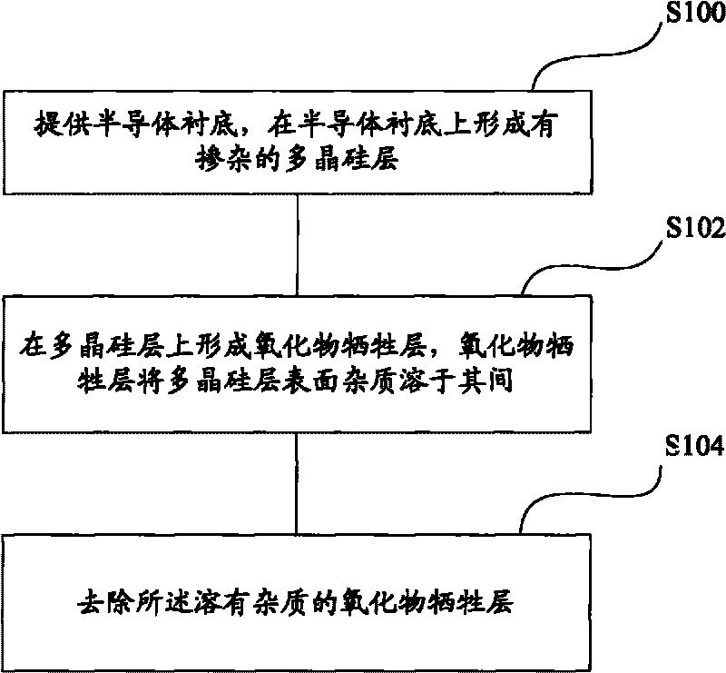
[0027] The inventors found that in the process of manufacturing semiconductor devices, when the polysilicon layer is formed, the surface of the silicon chip will be damaged by impurities (such as microparticles, fine fibers, carbon-containing organic matter, oil stains, SiH 4 Contamination of impurities in semiconductors, etc.) causes surface defects, affects the electrical properties of semiconductor devices, and leads to a decline in yield.

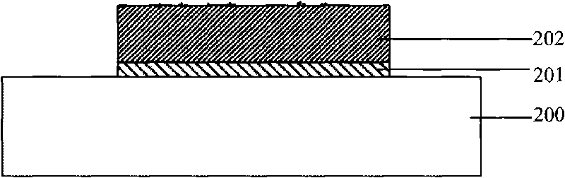
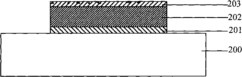
[0028] Therefore, in the manufacture of semiconductor devices, in order to prevent the above-mentioned defects, especially surface impurities, from affecting the product yield. The invention provides a method for eliminating surface defects of a semiconductor device, comprising: providing a semiconductor substrate, on which a doped polysilicon layer is formed, and impurities are attached to the surface of the polysilicon layer; forming an oxide sacrificial layer on which the impurity is dissolved; and removing the oxide sacrificial laye...


PUM

PropertyMeasurementUnit
thicknessaaaaaaaaaa
thicknessaaaaaaaaaa
thicknessaaaaaaaaaa

Abstract

The invention relates to a method for eliminating the surface defect of a semiconductor device and a semiconductor device. The method for eliminating the surface defect of a semiconductor device comprises the following steps of: providing a semiconductor substrate and forming an impure polycrystalline silicon layer on the semiconductor substrate, wherein impurities are adhered to the surface of the polycrystalline silicon layer; forming an oxide sacrificial layer on the polycrystalline silicon layer, wherein the impurities are dissolved in the oxide sacrificial layer; and removing the oxide sacrificial layer in which the impurities are dissolved. By removing the impurities originally attached to the surface of the semiconductor element, the pollution to the subsequent process is reduced, and the fine rate of the products is relatively raised.

Description

technical field [0001] The invention relates to the technical field of semiconductor manufacturing, in particular to a method for eliminating surface defects of a semiconductor device and the semiconductor device. Background technique [0002] At present, in the semiconductor process, the feature size of components is getting smaller and smaller, so the corresponding process requirements for semiconductors are getting higher and higher. Among them, the control of impurities in the process is a key to controlling the yield of devices. Factors are a big challenge for the semiconductor process. [0003] In the integrated circuit manufacturing process, polysilicon thin film plays a very important role. In CMOS circuits, heavily doped polysilicon is used instead of metal aluminum as the gate material of MOS transistors, which can realize the automatic arrangement of source, drain and gate, which greatly reduces the influence of Miller capacitance, which is beneficial to improve ...

Claims


Application Information

Patent Timeline
Patent Type & Authority Applications(China)
IPC IPC(8): H01L21/322
Inventor 韩秋华杜珊珊黄怡赵林林
Owner SEMICON MFG INT (SHANGHAI) CORP
Why Eureka
Try Eureka