Fully-automatic aligning high-pressure N-shaped DMOS device and manufacturing method thereof

A self-aligned, N-type technology, used in semiconductor/solid-state device manufacturing, semiconductor devices, electrical components, etc., can solve problems such as difficult to obtain, never had self-aligned drain applications, small on-resistance, etc. Achieve the effect of breaking through the limitation of process size, reducing size, and reducing on-resistance

Active Publication Date: 2010-06-23
SHANGHAI HUAHONG GRACE SEMICON MFG CORP
View PDF0 Cites 13 Cited by
  • Summary
  • Abstract
  • Description
  • Claims
  • Application Information

AI Technical Summary

Problems solved by technology

The registration accuracy of multiple photolithography determines that it is impossible to minimize the size of DMOS devices by using this traditional process method, so it

Method used


Image

  • Fully-automatic aligning high-pressure N-shaped DMOS device and manufacturing method thereof
  • Fully-automatic aligning high-pressure N-shaped DMOS device and manufacturing method thereof
  • Fully-automatic aligning high-pressure N-shaped DMOS device and manufacturing method thereof

Examples


Embodiment Construction

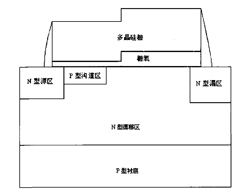
[0025] The key to the method for making a fully self-aligned N-type DMOS device in the BCD process flow of the present invention is to use a fully self-aligned process to realize the N-type DMOS device, so that the tertiary photoelectric process of the channel, the drift region and the drain is omitted. engraving, and finally realize the minimization of device size.

[0026] The process of the specific implementation of the method of the present invention is:

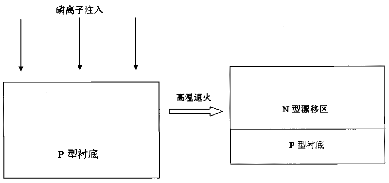
[0027] Step 1, see figure 2 As shown, high-energy phosphorus ion implantation is performed on the entire N-type DMOS device region on the P-type substrate, and high-temperature annealing is performed to finally form an N-type drift region on the P-type substrate. Phosphorus ion implantation dose at 1×10 13 cm -2 to 2×10 13 cm -2 , the implantation energy is 1000keV to 2000keV, the annealing temperature is 1500°C to 1800°C, and the annealing time is 1 hour to 3 hours.

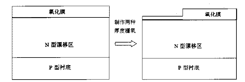
[0028] Step two, see image 3 As shown, a f...


PUM


Abstract

The invention discloses a method for manufacturing a fully-automatic aligning high-pressure N-shaped DMOS device (Diffused metal silicon oxide semiconductor field effect transistor), which comprises the following steps: injecting phosphorus with large energy in a whole N-shaped DMOS area and pushing at a high temperature to form an N-shaped drift region; injecting large-angle boron from a source port of a P-shaped channel after a polysilicon gate is etched and compensating the formed N-shaped drift region; causing the polysilicon gate to cover the whole N-shaped drift region; adopting a heterogeneous gate oxidation layer, adopting the conventional thin gate oxidation layer in a P-shaped channel region and manufacturing a thick gate oxidation layer on the N-shaped drift region nearby a drain electrode. The invention discloses a dully-automatic aligning high-pressure N-shaped DMOS device. The invention can achieve the minimum dimension of the N-shaped DMOS device and obtain a minimum on-state resistance.

Description

technical field [0001] The invention relates to the field of semiconductor integrated circuits, in particular to a method for manufacturing a fully self-aligned high-voltage N-type DMOS device in a BCD process flow. The invention also relates to a fully self-aligned high-voltage N-type DMOS device. Background technique [0002] The BCD (bipolar-CMOS-DMOS) process has a wide range of application values ​​in power management, among which high-voltage DMOS devices are the most important device types. From the perspective of reducing chip power consumption as much as possible, the DMOS device is required to have a small on-resistance under the premise of ensuring the working voltage, so the lateral size of the DMOS device should be reduced as much as possible. However, most of the current DMOS devices are manufactured using non-self-aligned process methods, such as forming channels by channel lithography, defining drift regions by lithography, forming drift regions between the ...

Claims


Application Information

Patent Timeline
IPC IPC(8): H01L21/336H01L29/78H01L29/423H01L29/10
Inventor 钱文生
Owner SHANGHAI HUAHONG GRACE SEMICON MFG CORP
Why Eureka
Try Eureka