Chip scale package structure of CMOS (complementary metal-oxide-semiconductor) image sensor and packaging method

An image sensor and chip-level packaging technology, which is applied in the semiconductor field, can solve the problems of a large number of connecting wires, affecting the freedom of connecting wire layout, and it is difficult to reduce the packaging area, so as to improve efficiency and reduce defect dislocations.

Active Publication Date: 2010-06-23
SEMICON MFG INT (SHANGHAI) CORP
View PDF1 Cites 12 Cited by
  • Summary
  • Abstract
  • Description
  • Claims
  • Application Information

AI Technical Summary

Problems solved by technology

For high-pixel CMOS sensors, the number of connection lines is huge, and the use of solder technology not only affects the freedom of the entire conne

Method used


Image

  • Chip scale package structure of CMOS (complementary metal-oxide-semiconductor) image sensor and packaging method
  • Chip scale package structure of CMOS (complementary metal-oxide-semiconductor) image sensor and packaging method
  • Chip scale package structure of CMOS (complementary metal-oxide-semiconductor) image sensor and packaging method

Examples


no. 1 approach

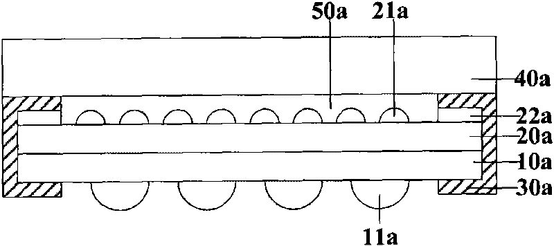
[0016] The first embodiment of the present invention provides a chip-level packaging method for a CMOS semiconductor image sensor, including providing a semiconductor substrate, forming a photoelectric conversion layer in the semiconductor substrate, forming a wiring layer on the surface of the photoelectric conversion layer, and the wiring layer Discrete connection pads are formed on the surface; an adhesion layer is formed on the surface of the wiring layer, and the adhesion layer covers the connection pads; a supporting layer is formed on the surface of the adhesion layer; the semiconductor substrate is thinned until the photoelectric conversion layer is exposed, and the photoelectric conversion layer The pixel elements distributed in an array and the connecting layer between the pixel elements are formed on it, the height of the connecting layer is higher than that of the pixel elements; a light-transmitting layer is formed on the connecting layer, and the light-transmitting...

no. 2 approach

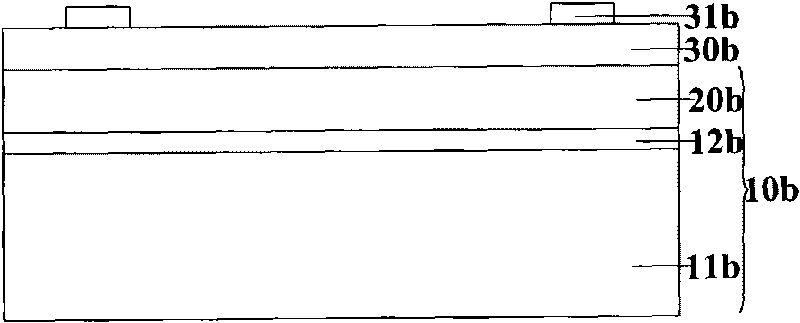
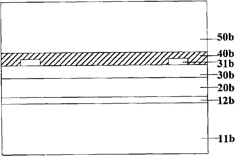
[0039] The second embodiment of the present invention provides a chip-level packaging method for a CMOS semiconductor image sensor, including providing a semiconductor substrate, forming a photoelectric conversion layer in the semiconductor substrate, forming a wiring layer on the surface of the photoelectric conversion layer, and the wiring layer Discrete connection pads are formed on the surface; an adhesion layer is formed on the surface of the wiring layer, and the adhesion layer covers the connection pads; a supporting layer is formed on the surface of the adhesion layer; the semiconductor substrate is thinned until the photoelectric conversion layer is exposed, and the photoelectric conversion layer The pixel elements distributed in an array and the connection layer between the pixel elements are formed on it, and the height of the connection layer is higher than the pixel elements; a light-transmitting layer is formed on the connection layer, and the light-transmitting la...


PUM

PropertyMeasurementUnit
Thicknessaaaaaaaaaa
Thicknessaaaaaaaaaa
Thicknessaaaaaaaaaa

Abstract

The invention discloses a chip scale package structure of a CMOS (complementary metal-oxide-semiconductor) image sensor and a packaging method. The chip scale package structure of the CMOS image sensor comprises a wiring layer, a photoelectric conversion layer, a pixel element array, a connection layer, a photic zone, an adhesion layer, a supporting layer, a conductive plug adapter, a bonding pad and solder joints, wherein the wiring layer equipped with a split connection pad; the photoelectric conversion layer is positioned on the surface of the wiring layer, and the photoelectric conversion layer and the connection pad are positioned at an opposite surface of the wiring layer; the pixel element array is positioned on the photoelectric conversion layer; the connection layer is positioned on the photoelectric conversion layer for separating the pixel element array and is higher than a pixel element; the photic zone is positioned on the connection layer and covers the pixel element, a cavity is formed on a pixel element area, and the adhesion layer is positioned on the wiring layer and covers the connection pad; the supporting layer is positioned on the adhesion layer; the conduction plug adapter penetrates through the supporting layer and the adhesion layer and expose the connection pad; and the bonding pad is positioned on the conductive plug adapter, and the solder spots are positioned on the surface of the bonding pad. The invention effectively improves the performance and the integration level of a device.

Description

technical field [0001] The invention relates to the technical field of semiconductors, in particular to a chip-level packaging structure and packaging method of a CMOS image sensor. Background technique [0002] At present, the charge coupled device (CCD) is the main practical solid-state image sensing device, which has the advantages of low read noise, large dynamic range, and high response sensitivity. The disadvantage of Complementary-Metal-Oxide-Semiconductor (CMOS) technology compatibility is that it is difficult to achieve single-chip integration with CCD-based image sensors. [0003] The CMOS image sensor (CMOS Image sensor, CIS) is produced in order to overcome the complex manufacturing process and high energy consumption of the charge-coupled device (CCD). MOS transistors. Due to the use of CMOS technology, CIS can integrate the pixel unit array and peripheral circuits on the same chip. Compared with CCD, CIS has the advantages of small size, light weight, low pow...

Claims


Application Information

Patent Timeline
IPC IPC(8): H01L21/50H01L21/60H01L27/146H01L23/48
CPCH01L2224/13
Inventor 三重野文健鲍震雷
Owner SEMICON MFG INT (SHANGHAI) CORP
Why Eureka
Try Eureka