Avalanche photodiode

An avalanche photoelectric and diode technology, applied in circuits, electrical components, semiconductor devices, etc., can solve difficult problems and achieve low power consumption

Inactive Publication Date: 2010-06-23
MITSUBISHI ELECTRIC CORP
View PDF6 Cites 7 Cited by
  • Summary
  • Abstract
  • Description
  • Claims
  • Application Information

AI Technical Summary

Problems solved by technology

However, when crystal growth is performed by the metalorganic vapor phase growth (MO-CVD) method or the molecular beam epitaxy (MBE) method, even if impurities are not intentionally added, 10 15 cm -3 level of n-type or p-type conductivity, it is very difficult to precisely control the carrier concentration

Method used


Image

  • Avalanche photodiode
  • Avalanche photodiode
  • Avalanche photodiode

Examples


Embodiment approach 1

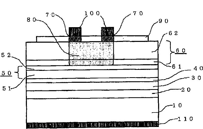
[0026] figure 1 is a schematic cross-sectional view of an avalanche photodiode in Embodiment 1 for implementing the present invention. In this embodiment, the first conductivity type is n-type and the second conductivity type is p-type for description.

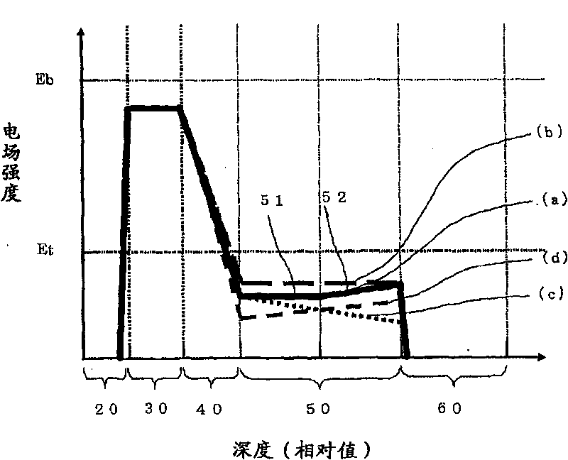
[0027] figure 1 Among them, a low-resistance n-type InP material substrate 10 is formed on the first main surface with a film thickness of 0.1-1 μm and a carrier concentration of 1-5×10 18 cm -3 , The buffer layer 20 of n-type InP material. Formed on the buffer layer 20 with a film thickness of 0.1 to 0.5 μm and a carrier concentration of 0.1 to 3×10 15 cm -3 . The avalanche multiplication layer 30 of undoped AlInAs material. Formed on the avalanche multiplication layer 30 with a film thickness of 0.01 to 0.1 μm and a carrier concentration of 0.1 to 1×10 18 cm -3 . The electric field adjustment layer 40 made of p-type InP material. On the electric field adjusting layer 40, an undoped light absorbing layer 51 of GaInAs...

Embodiment approach 2

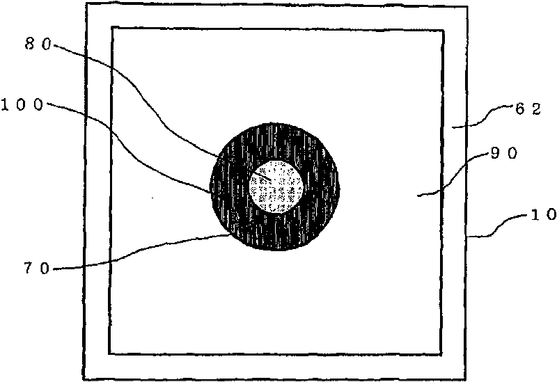
[0076] Figure 11 is a cross-sectional view showing a schematic structure of an avalanche photodiode according to Embodiment 2 of the present invention. exist Figure 11 In Embodiment 1, the window layer 60 having a double-layer structure is formed with one layer of p-type window layer 63, an etching stop layer 160 is provided between the p-type window layer 63 and the light absorbing layer 50, and the p-type window layer 63 Except that island-shaped annular grooves 150 having a diameter of 20 to 100 μm and having a desired light-receiving size are provided thereon, it is the same as Embodiment 1, and thus detailed description thereof will be omitted.

[0077] Here, the p-type window layer 63 is an AlInAs material with a thickness of 0.5-2.0 μm, and a carrier concentration of 0.3-3×10 16 cm -3 ; The etch stop layer 160 has a film thickness of 0.01-0.05 μm and a carrier concentration of 0.3-3×10 16 cm -3 , n-type InP material. In addition, the carrier concentration of the...


PUM


Abstract

The conventional avalanche photodiodes are not easy to be fabricated, because if the light absorption layer is in un-doped type, the bias voltage during operation is high, and if the light absorption layer is only slightly doped, the doping amount thereof is hard to be controlled. To this end, the invention provides an avalanche photodiode comprises: a substrate of a first conductivity type; and an avalanche multiplication layer, a light absorption layer, and a window layer which are sequentially laminated from the substrate, wherein a part of the window layer is a region of a second conductivity type, and the light absorption layer includes a first light absorption layer, and a second light absorption layer which has higher electric conductivity than electric conductivity of the first light absorption layer.

Description

technical field [0001] The present invention relates to a photodiode that improves light receiving sensitivity by utilizing a phenomenon called avalanche multiplication, that is, an avalanche photodiode used in optical fiber communication and the like. Background technique [0002] An avalanche photodiode has a light absorption region and an avalanche multiplication region. If light is incident on the avalanche photodiode in a state where a reverse bias voltage is applied, the light is absorbed in the light absorption region and electron-hole pairs are generated, and the photocarriers generated in the light absorption region are The avalanche multiplication region is avalanchely multiplied by ionized collisions. Avalanche photodiodes that receive near-infrared light are required to have high reliability, low power consumption, and high efficiency in addition to high sensitivity and high-speed response in order to be used in optical fiber communications. [0003] As an aval...

Claims


Application Information

Patent Timeline
Patent Type & Authority Applications(China)
IPC IPC(8): H01L31/107H01L31/0256H01L31/18
CPCH01L31/1075
Inventor 柳生荣治石村荣太郎中路雅晴
Owner MITSUBISHI ELECTRIC CORP
Why Eureka
Try Eureka