Zero drift compensation method of Hall magnetic sensor

A zero-point drift, magnetic sensor technology, applied in instruments, electric solid-state devices, semiconductor devices, etc., can solve the problems of poor ohmic contact of electrodes, not easy to miniaturize magnetic sensors, intelligent development, uneven temperature, etc.

Inactive Publication Date: 2010-07-07
HEILONGJIANG UNIV
View PDF0 Cites 17 Cited by
  • Summary
  • Abstract
  • Description
  • Claims
  • Application Information

AI Technical Summary

Problems solved by technology

[0002] At present, when the known Hall magnetic sensor is applied with a magnetic field B=0, the Hall output voltage VH is not equal to zero due to factors such as geometric asymmetry of the Hall electrode, poor ohmic contact of the electrode, uneven resistivity, and uneven temperature, resulting in zero bit error VHO
In order to eliminate the zero error, an external compensation circuit is mainly used to compensate the zero drift. This method is not easy for the magnetic sensor to develop in the direction of miniaturization and intelligence.

Method used


Image

  • Zero drift compensation method of Hall magnetic sensor
  • Zero drift compensation method of Hall magnetic sensor
  • Zero drift compensation method of Hall magnetic sensor

Examples


Embodiment 1

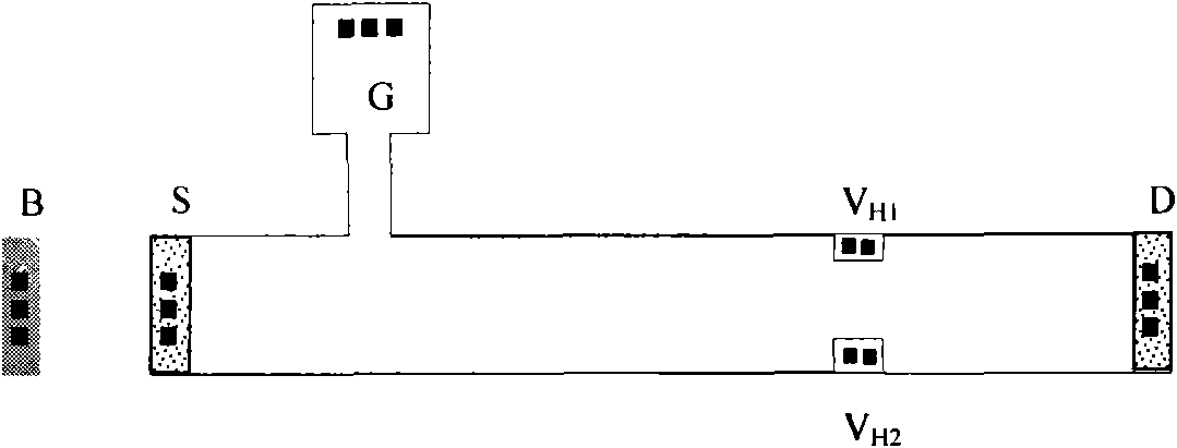
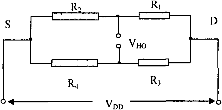
[0028] The method of compensating for the zero drift of the Hall magnetic sensor is to make the MOSFET Hall Hall magnetic sensor through the CMOS process. The four equivalent resistance resistances of the channel of the Hall magnetic sensor change with the external gate voltage.

[0029] The CMOS process includes flushing, first oxidation, first photolithography, second oxidation, P-type doping, third oxidation, and 215 photolithography.

[0030] See attached figure 1 , N-type double-sided polished high-resistance (ρ>100Ω·cm) single crystal silicon wafer with a thickness of 450 μm, boiled with concentrated sulfuric acid until white smoke, rinsed with a large amount of deionized water after cooling, and then cleaned with cleaning solution DZ-1 , DZ-2 were washed twice each, rinsed with a large amount of deionized water, and dried in a dryer;

[0031] Put the cleaned monocrystalline silicon wafer into a high-temperature oxidation furnace for primary oxidation, and use a thermal...


PUM


Abstract

The invention provides a zero drift compensation method of a Hall magnetic sensor. At present, the existing Hall magnetic sensor has the defects that the output voltage VH of the Hall magnetic sensor is not equal to zero, and the zero error VHO is generated because of factors such as unsymmetrical geometric positions of Hall electrodes, poor ohmic contact of the electrodes, nonuniform electric resistivity, nonuniform temperature and the like when the external magnetic filed B is equal to zero. In order to eliminate the zero error, the invention mainly adopts an external compensation circuit for compensating the zero drift. When the method is used, the magnetic sensor is difficult to develop in the directions of miniaturization and intelligentization. The invention uses a CMOS process for manufacturing grooves of the MOSFET Hall magnetic sensor so that the resistance values of four equivalent resistors are changed along with the external grid voltage. The invention is applicable to the fields of medicine, automobiles and the like.

Description

Technical field: [0001] The invention relates to a zero position compensation method for the MOSFET Hall magnetic sensor by adjusting the equivalent resistance of the conduction channel of the MOSFET Hall magnetic sensor through grid bias voltage. Background technique: [0002] At present, when the known Hall magnetic sensor is applied with a magnetic field B=0, the Hall output voltage VH is not equal to zero due to factors such as geometric asymmetry of the Hall electrode, poor ohmic contact of the electrode, uneven resistivity, and uneven temperature, resulting in zero Bit Error VHO. In order to eliminate the zero error, an external compensation circuit is mainly used to compensate the zero drift. This method is not easy for the magnetic sensor to develop in the direction of miniaturization and intelligence. Invention content: [0003] The purpose of the present invention is to provide a method for compensating the zero point drift that is affected by the performance of...

Claims


Application Information

Patent Timeline
Patent Type & Authority Applications(China)
IPC IPC(8): H01L21/82H01L21/8238H01L27/22G01R33/07
Inventor 赵晓锋温殿忠
Owner HEILONGJIANG UNIV
Why Eureka
Try Eureka