AlGaInP system LED with electron hole dual limitation and preparation method thereof

An electron-hole, dual technology, applied in the field of optoelectronics, can solve the problems of poor thermal characteristics, low optical power, low luminous efficiency, etc., and achieve the effects of low cost, high repeatability and simple process

Inactive Publication Date: 2010-07-07
Shandong Huaguang Optoelectronics Co. Ltd.
View PDF1 Cites 19 Cited by
  • Summary
  • Abstract
  • Description
  • Claims
  • Application Information

AI Technical Summary

Problems solved by technology

[0005] The present invention aims at the problems of low luminous efficiency, small optical power, poor thermal characteristics and the like existing in the structure of the existing AlGaInP (aluminum gallium indium phosphide) series LED, and provides an electron-hole double LED with improved luminous efficiency and light extraction efficiency. The limited AlGaInP series LED can significantly improve the internal current distribution of the chip, make the current more and more evenly distributed in the light emitting area, and at the same time improve the light output on the side of the tube core, greatly improving the light efficiency and life of the LED

Method used


Image

  • AlGaInP system LED with electron hole dual limitation and preparation method thereof
  • AlGaInP system LED with electron hole dual limitation and preparation method thereof
  • AlGaInP system LED with electron hole dual limitation and preparation method thereof

Examples


Embodiment Construction

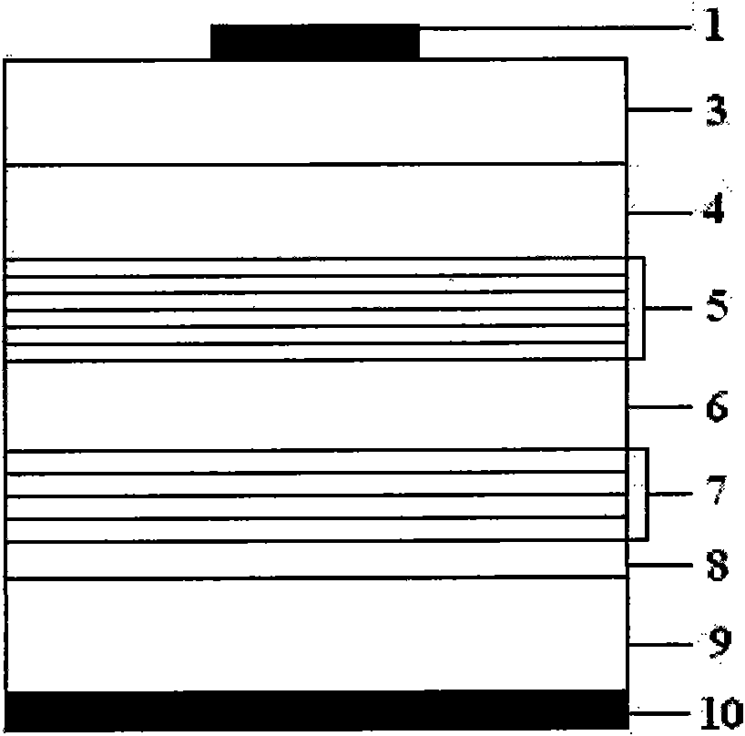
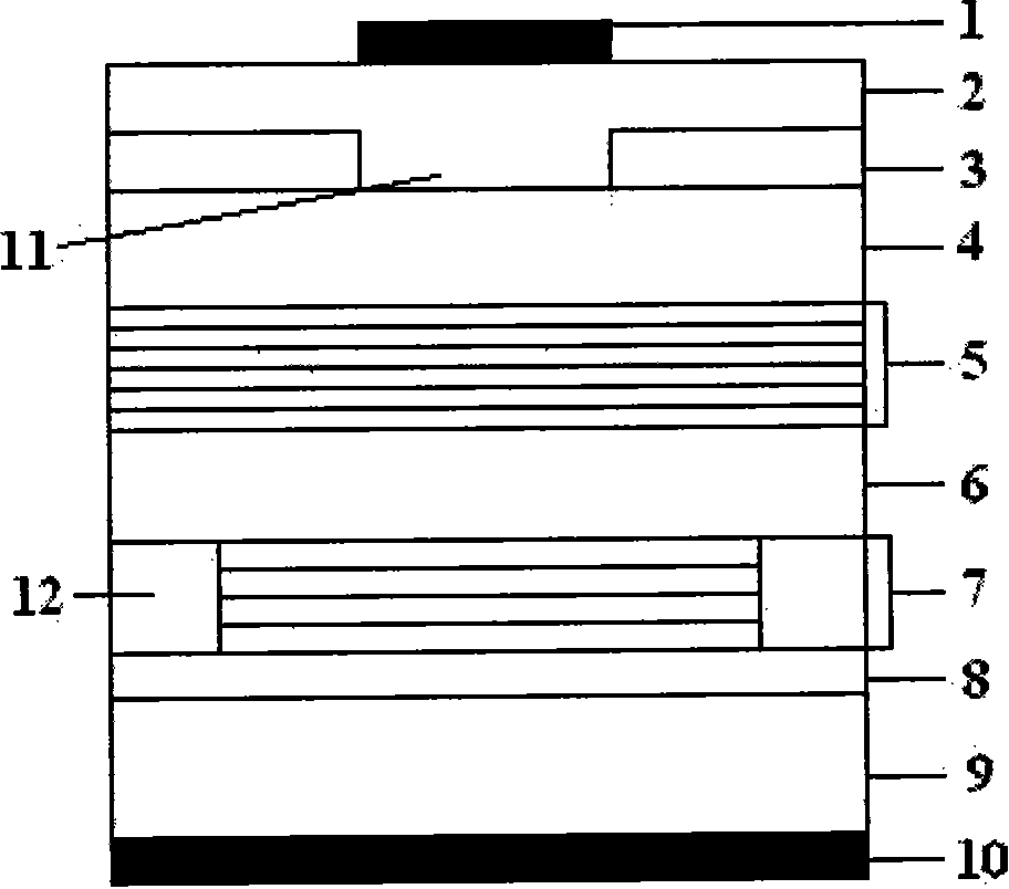
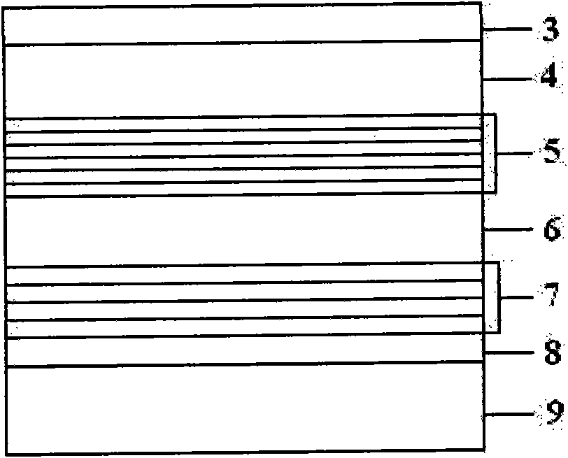
[0027] The AlGaInP LED with double restriction of electrons and holes of the present invention has a chip structure such as figure 2 As shown, from top to bottom, it includes an upper electrode 1, an ITO conductive light-transmitting layer 2, a GaP window layer 3, an upper confinement layer 4, an active region 5, a lower confinement layer 6, a Bragg reflective layer 7, a buffer layer 8, and a substrate 9 and lower electrode 10. The GaP window layer 3 is provided with an etching area corresponding to the shape and position of the upper electrode 1. The etching area is as deep as the upper surface of the upper confinement layer 4. The ITO conductive light-transmitting layer 2 extends from the etching area on the GaP window layer 3 to the upper surface. On the upper surface of the confinement layer 4, a Schottky contact is formed, and a current blocking region 11 is formed. The maximum carrier concentration of ITO conductive light-transmitting layer 2 reaches 10 21 cm -3 Order of...


PUM

PropertyMeasurementUnit
thicknessaaaaaaaaaa
thicknessaaaaaaaaaa

Abstract

The invention provides an AlGaInP system LED with the electron hole dual limitation and a preparation method thereof. An upper electrode, an ITO conductive light transmission layer, a GaP window layer, an upper limiting layer, an active region, a lower limiting layer, a Bragg reflecting layer, a buffer layer, a substrate and a lower electrode vertically and sequentially grow in a laminated way on a chip structure of the LED from top to bottom, wherein the ITO conductive light transmission layer extends from the GaP window layer to the upper surface of the upper limiting layer, and both sides of the Bragg reflecting layer are provided with oxidizing insulation regions. The preparation method comprises the following steps: (1) growing epitaxial materials; (2) etching current baffle regions; (3) carrying out vapor deposition on ITO transparent conductive films; (4) manufacturing the upper electrode and the lower electrode; (5) carrying out oxidization; and (6) separating pipe cores and carrying out encapsulation. The invention forms the Schottky contact with the upper limiting layer through the ITO transparent conductive films, so the current baffle layer is formed. The process is simple, the repetitiveness is high, and in addition, the cost is low, so the luminous efficiency and the light extraction efficiency of the LED are improved.

Description

Technical field [0001] The invention relates to a structure of an AlGaInP (aluminum gallium indium phosphorous) LED (light emitting diode) and a preparation method thereof, and belongs to the technical field of optoelectronics. Background technique [0002] LED has the advantages of small size, long life and low power consumption. Among them, the AlGaInP system LED prepared on GaAs substrate has superior performance in the yellow-green, yellow, orange and red bands. It is currently widely used in RGB three-color full-color displays, white Light sources, traffic lights, urban lighting projects, automotive lamps and other fields have broad application prospects. [0003] At present, the structure of ordinary AlGaInP LED chips is as figure 1 As shown, from bottom to top, it includes a lower electrode 10, a substrate 9, a buffer layer 8, a Bragg reflective layer 7, a lower confinement layer 6, an active region 5, an upper confinement layer 4, a current spreading layer (GaP window layer...

Claims


Application Information

Patent Timeline
Patent Type & Authority Applications(China)
IPC IPC(8): H01L33/14C23C16/44
Inventor 李树强徐现刚张新吴作贵
Owner Shandong Huaguang Optoelectronics Co. Ltd.
Why Eureka
Try Eureka