Method for preparing monodispersed cuprous sulfide semiconductor nanocrystalline

A technology of cuprous sulfide and semiconductor, which is applied in the direction of copper sulfide, nanostructure manufacturing, nanotechnology, etc., and can solve problems such as complex operation

Inactive Publication Date: 2010-07-21
INST OF SEMICONDUCTORS - CHINESE ACAD OF SCI
View PDF0 Cites 7 Cited by
  • Summary
  • Abstract
  • Description
  • Claims
  • Application Information

AI Technical Summary

Problems solved by technology

However, these methods are complex to operate, require multi-step reactions, and require the preparation of metal precursors in advance, etc.

Method used


Image

  • Method for preparing monodispersed cuprous sulfide semiconductor nanocrystalline
  • Method for preparing monodispersed cuprous sulfide semiconductor nanocrystalline
  • Method for preparing monodispersed cuprous sulfide semiconductor nanocrystalline

Examples


preparation example Construction

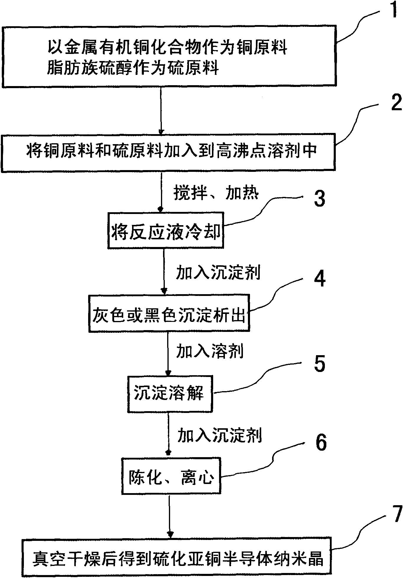
[0027] see figure 1 Shown, the present invention provides a kind of preparation method of monodisperse cuprous sulfide semiconductor nanocrystal, comprises the steps:

[0028] Step 1: Use metal organic copper compounds as copper raw materials, aliphatic mercaptans as sulfur raw materials, no need to prepare precursors of copper raw materials in advance, and the reaction operation is simple; wherein, the metal organic copper compounds are copper acetylacetonate, copper acetate or hard One of copper fatty acid; the aliphatic mercaptan is one of dodecyl mercaptan, cetyl mercaptan or octadecyl mercaptan;

[0029] Step 2: adding the copper raw material and the sulfur raw material together into a high boiling point solvent, stirring evenly, and performing a heating reaction to obtain a reaction liquid, which gradually changes from turbid to a clear solution, and then becomes turbid again; wherein, the The reaction temperature is 180-240°C, and the reaction time is 10 minutes-4 hour...

Embodiment 1

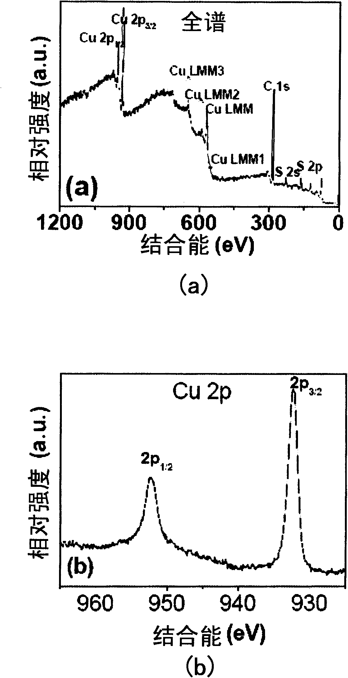
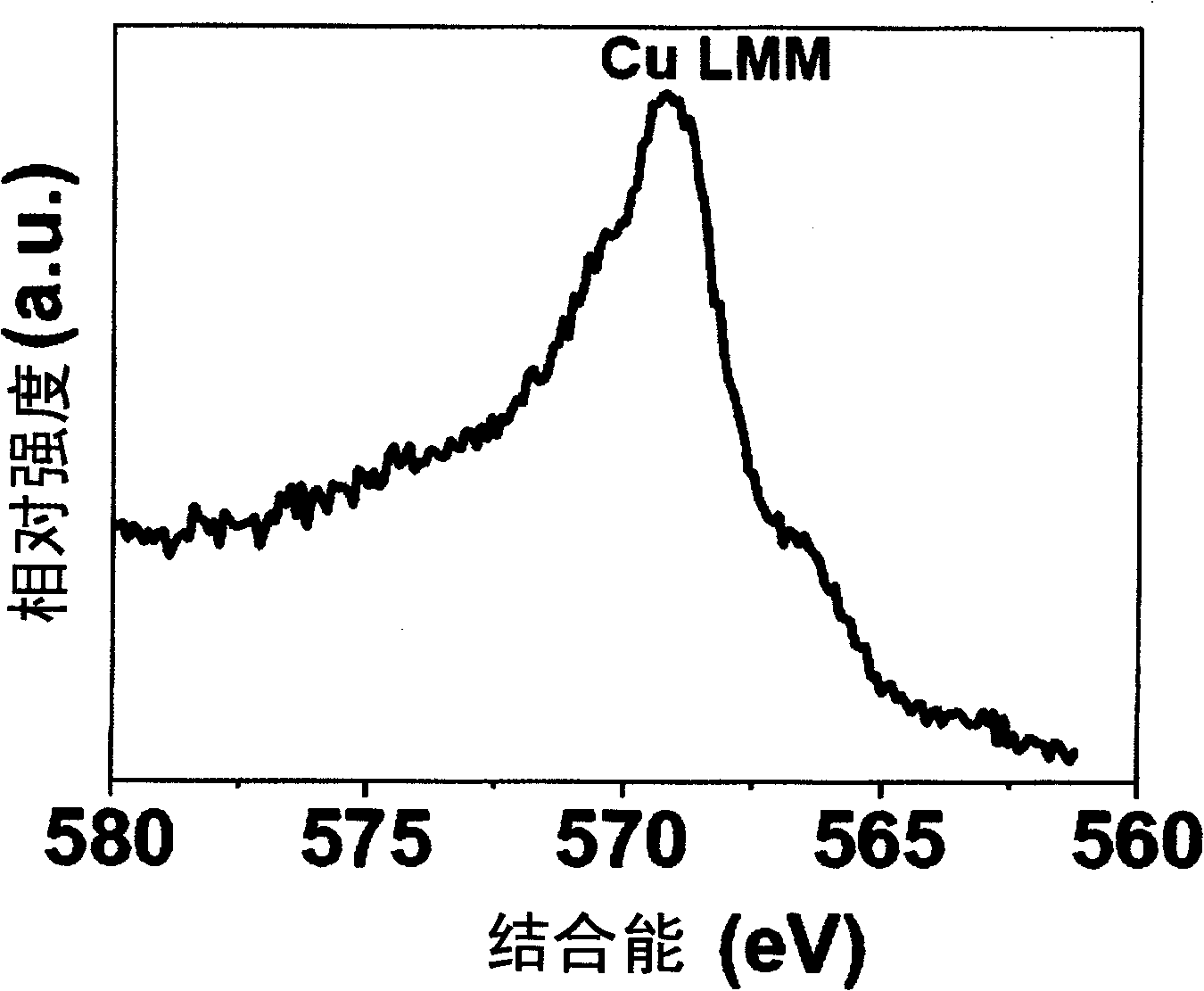
[0036] 3 millimoles of copper acetylacetonate and 10 milliliters of dodecanethiol were added to 20 milliliters of oleylamine, and the reaction solution was slowly heated to 200 ° C, and reacted for 120 minutes under magnetic stirring. After the reaction was completed, it was naturally cooled to room temperature. Add ethanol to the reaction solution for precipitation, then add chloroform solvent to the precipitate to dissolve to obtain a solution, then add ethanol to the solution, after aging and centrifugation, vacuum-dry the obtained sample at 70°C After 6 hours, cuprous sulfide nanocrystals were obtained.

[0037] figure 2 and image 3 are respectively the X-ray photoelectron spectrum and the Auger electron spectrum of the cuprous sulfide semiconductor nanocrystal prepared in this embodiment, wherein figure 2 (b) Energy spectrum of Cu 2p and image 3 The Auger electron spectrum in all proves that the valence state of Cu element is +1. Figure 4 It is the X-ray powder d...

Embodiment 2

[0039] 3 millimoles of copper acetylacetonate and 5 milliliters of dodecanethiol were jointly added in 25 milliliters of oleylamine, and all the other operations were the same as in Example 1.


PUM

PropertyMeasurementUnit
diameteraaaaaaaaaa
diameteraaaaaaaaaa

Abstract

The invention relates to a method for preparing monodispersed cuprous sulfide semiconductor nanocrystalline, comprising the following steps of: step 1, taking metal organic copper compounds as copper raw materials and aliphatic thiol as sulfur raw materials; step 2, adding the copper raw materials and the sulfur raw materials to a solvent with high boiling point, uniformly stirring the mixture, and carrying out heating reaction on the mixture to obtain a reaction liquid; step 3, cooling the reaction liquid to the room temperature; step 4, adding a precipitator to the reaction liquid to separate out gray or black precipitates; step 5, adding a solvent to the separated precipitates, and dissolving the precipitates to obtain a solution; step 6, adding the precipitator to the dissolved solution for aging and centrifugation; and step 7, drying in vacuum to obtain the cuprous sulfide semiconductor nanocrystalline.

Description

technical field [0001] The invention belongs to the field of synthesis methods of semiconductor nanocrystals, and in particular relates to a preparation method of monodisperse cuprous sulfide semiconductor nanocrystals. Background technique [0002] In the past ten years, semiconductor colloidal nanocrystals have attracted widespread attention from domestic and foreign scientists in basic research and applied research, such as the A.P. Alivisatos research group at the University of California, Berkeley, M.G.Bawendi at the Massachusetts Institute of Technology The research group and Li Yadong's research group at Tsinghua University have achieved outstanding research work in the synthesis and application of semiconductor nanocrystals. However, most of the research work is concentrated on the synthesis, optical properties, optoelectronic devices and biomarkers of semiconductor nanocrystals such as CdSe, CdS, PbS and PbSe. Due to the pollution of the environment by these semicon...

Claims


Application Information

Patent Timeline
Patent Type & Authority Applications(China)
IPC IPC(8): C01G3/12B82B3/00
Inventor 唐爱伟曲胜春王占国
Owner INST OF SEMICONDUCTORS - CHINESE ACAD OF SCI
Why Eureka
Try Eureka