Circuitry and method for reducing second and third-order nonlinearities

A third-order nonlinear, circuit technology, applied in the direction of improving amplifiers to reduce nonlinear distortion, electrical components, components of amplifying devices, etc., can solve problems such as no second-order nonlinear elimination discussion

Inactive Publication Date: 2010-07-21
TELEFON AB LM ERICSSON (PUBL)
View PDF3 Cites 2 Cited by
  • Summary
  • Abstract
  • Description
  • Claims
  • Application Information

AI Technical Summary

Problems solved by technology

without discussing the elimination of

Method used


Image

  • Circuitry and method for reducing second and third-order nonlinearities
  • Circuitry and method for reducing second and third-order nonlinearities
  • Circuitry and method for reducing second and third-order nonlinearities

Examples


Embodiment Construction

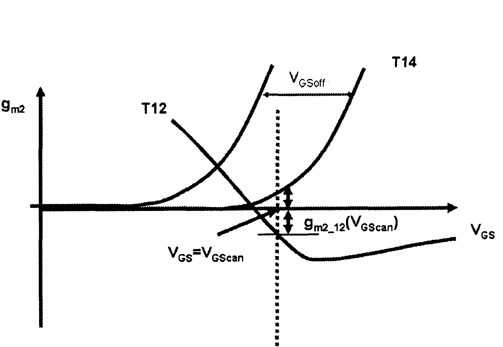
[0027] In operation, the transconductance of a transistor depends not only on the gate-source voltage but also on the drain-source voltage, as do the second- and third-order nonlinearities. In addition, transistor size and threshold voltage are also two important parameters to consider when dealing with transistor nonlinearity. With these conditions in mind, a circuit and method for eliminating second and third order nonlinearities is described below.

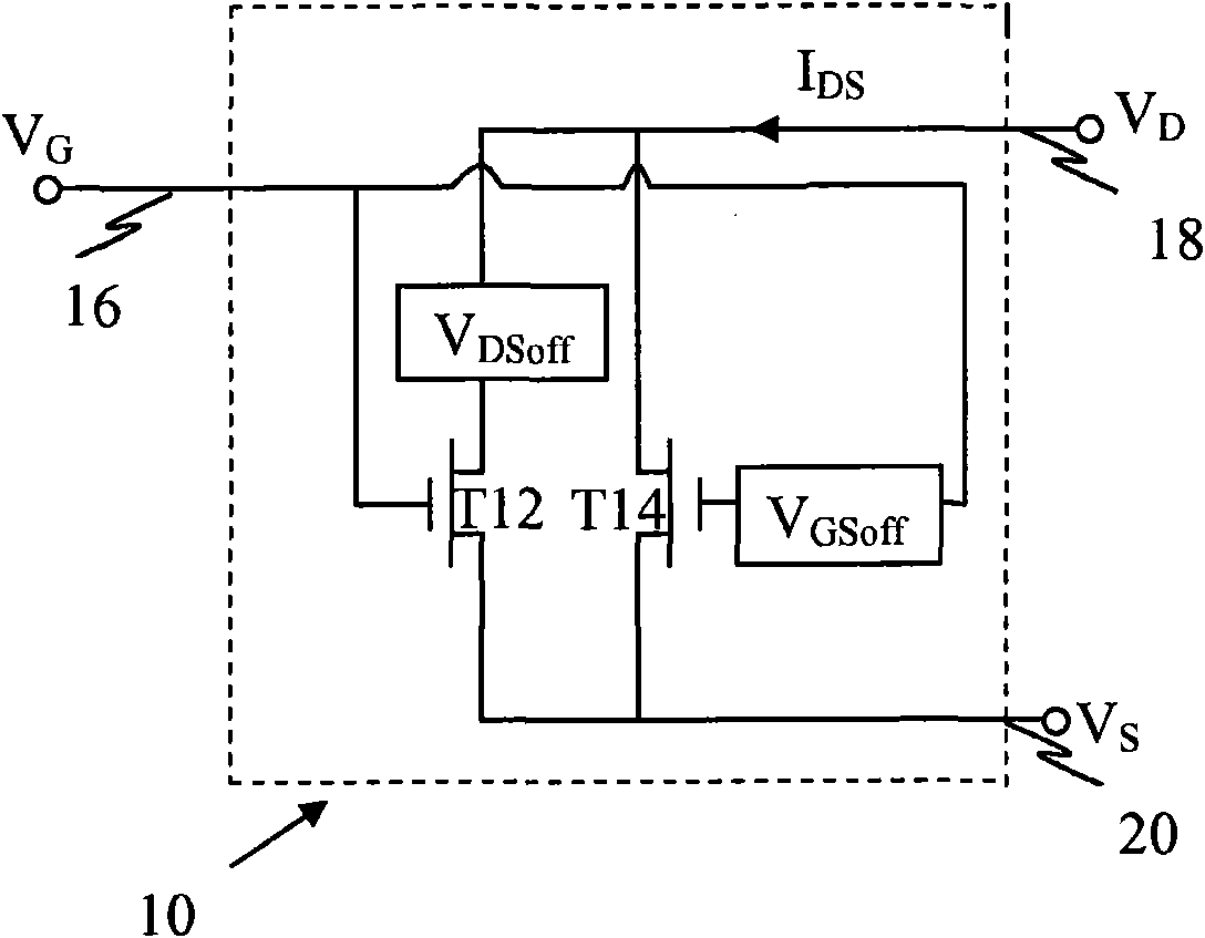
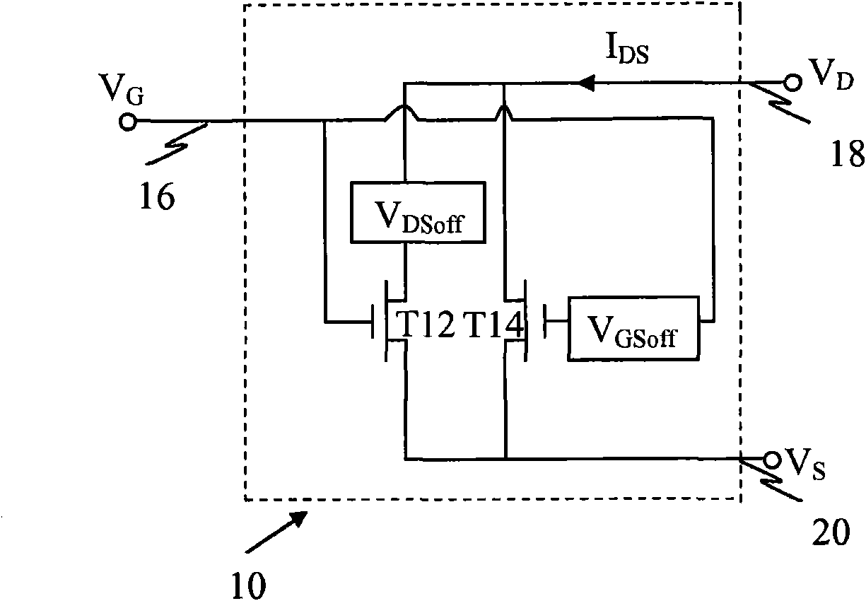
[0028] figure 1 A "composite" transistor circuit 10 is shown, formed by coupling a first transistor T12 in parallel with a second transistor T14 such that the two transistors T12 and T14 share a gate connection 16 , a drain connection 18 and a source connection 20 . (For a bipolar implementation of transistor circuit 10, these connections correspond to base, collector, and emitter connections, respectively.) Offset the gate bias of transistor T14 from the gate bias of transistor T12 by V GSoff . Offset the drain bias of tran...


PUM


Abstract

An electronic circuit (10) comprises at least two transistors (T12, T14) coupled in parallel, wherein the second transistor channel length is configured such that the threshold voltage of the second transistor (T14) is at a peak on a threshold voltage versus channel lengths curve arising from reverse short channel effects for a given semiconductor process. The first transistor (T12) is biased with a first gate-source voltage and a first drain-source voltage. The second transistor (T14) is biased with a second gate-source voltage and a second drain-source voltage. The first gate-source voltage and the second gate-source voltage are offset from each other by a gate-source voltage offset and the first drain-source voltage and the second drain-source voltage are offset from each other by a drain-source voltage offset. These bias conditions result in the transistors (T12, T14) operating in different regions so that the second and third-order nonlinearities of the transistors (T12, T14) substantially cancel each other out simultaneously.

Description

technical field [0001] The present invention relates generally to electronic circuits, and in particular to reducing second and third order nonlinearities of transistor devices in electronic circuits. Background technique [0002] In most communication circuits, linear signal amplification represents a core enabling function. For example, wireless communication transceivers employ linear signal amplification at various stages in their transmit and receive signal processing paths. More specifically, radio frequency (RF) based communication systems rely on linear amplification in mixer circuits, low noise amplifier circuits, power amplifier circuits, etc. to maintain signal fidelity and limit the generation of unwanted harmonic frequencies. However, the non-linear volt-ampere (IV) characteristics of semiconductor transistors (eg, bipolar or MOS transistors) represent a fundamental source of signal non-linearity in communication circuits that rely heavily on the use of such tr...

Claims


Application Information

Patent Timeline
IPC IPC(8): H03F1/32H03F3/21
CPCH03F3/211H03F2200/294H03F2200/492H03F2200/432H03F2200/456H03F1/3205H03F2200/453H03F3/195H03F2203/21178H03F2200/451
Inventor T·阿恩伯格
Owner TELEFON AB LM ERICSSON (PUBL)
Why Eureka
Try Eureka