
Plasma processing device and processing method thereof

A plasma and processing device technology, applied in the field of plasma processing devices, can solve the problems that the plasma density is easy to change, affect the uniformity and uniform distribution of substrate etching, and achieve increased plasma density, stable uniformity, Adjusting the Effects of Uniformity

Active Publication Date: 2010-07-28
ADVANCED MICRO FAB EQUIP INC CHINA
View PDF0 Cites 7 Cited by
  • Summary
  • Abstract
  • Description
  • Claims
  • Application Information

AI Technical Summary

Problems solved by technology

[0004] However, in the processing chamber of the plasma processing device, due to the different process parameters such as the type of etching gas, the gas pressure, and the power of the high-frequency voltage, the density of the generated plasma is very easy to change, and it is difficult to change the density around the substrate. Uniform distribution, affecting the uniformity of substrate etching

Method used


Image

  • Plasma processing device and processing method thereof
  • Plasma processing device and processing method thereof
  • Plasma processing device and processing method thereof

Examples


Embodiment 1

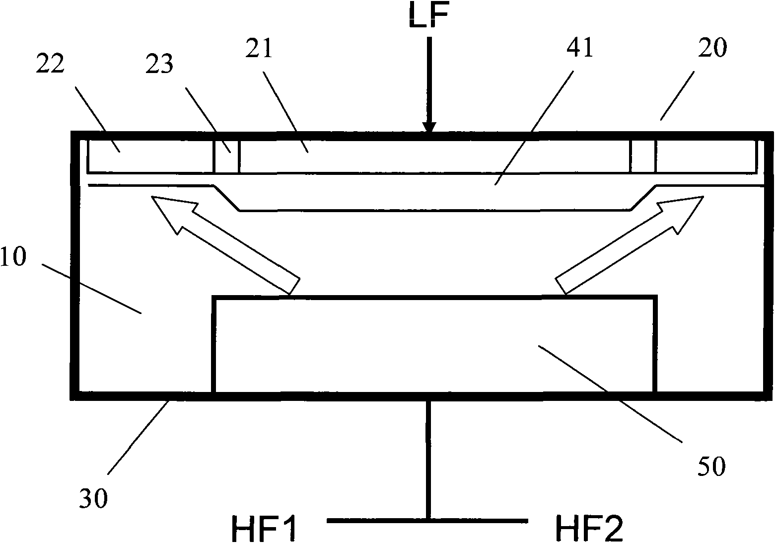
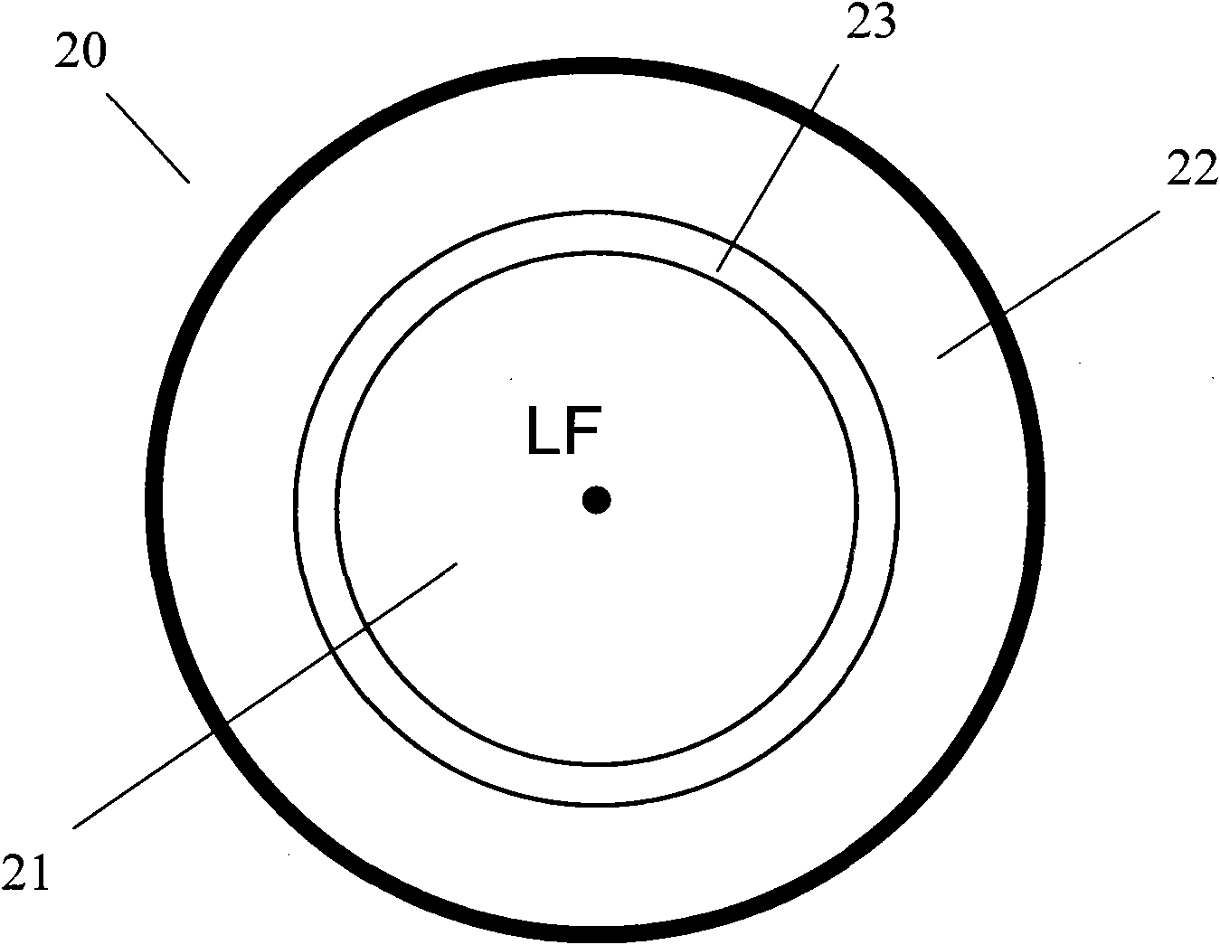
[0060] Please refer to figure 1 and figure 2 As shown, a plasma processing device provided by the present invention is used to generate gas plasma to react with the substrate 50 to realize etching and other processing of the substrate 50 . The capacitively coupled plasma processing device includes a processing chamber 10, an upper electrode 20 and a lower electrode 30 arranged in parallel in the processing chamber 10, an AC power supply LF connected to the upper electrode 20, and a first electrode connected to the lower electrode 30. RF power source HF1.

[0061] The processing chamber 10 is vacuumed, wherein a reactive gas for etching the substrate 50 is introduced, the reactive gas contains oxygen O 2 or nitrogen N 2 etching gas. The lower electrode 30 is horizontally arranged below the inside of the processing chamber 10 , and the substrate 50 to be processed is placed on the lower electrode 30 .

[0062] Corresponding to the lower electrode 30 , an upper electrode 20...

Embodiment 2

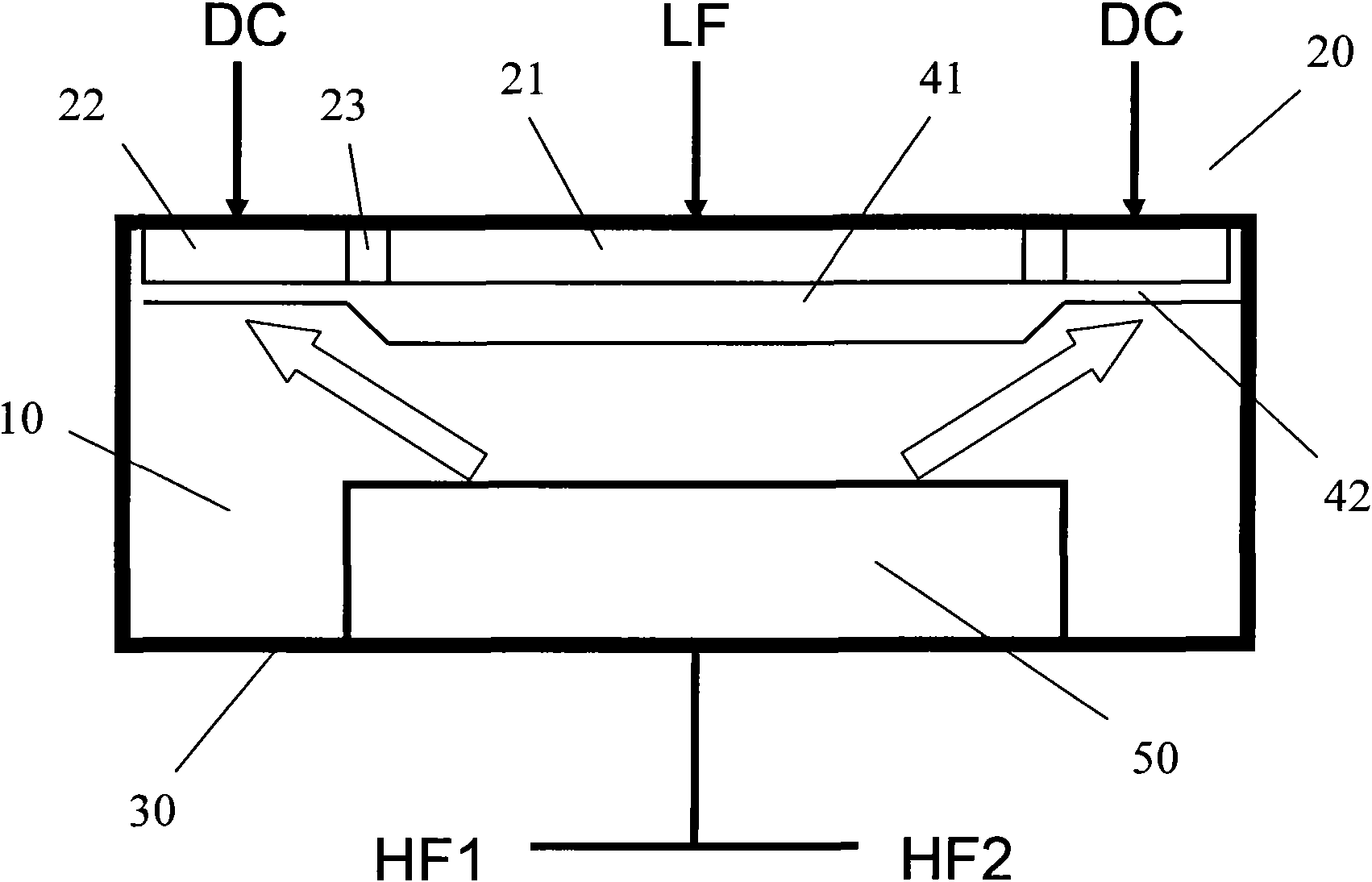
[0073] See image 3 As shown, this embodiment is similar to the overall structure of the plasma processing device provided in Embodiment 1, including a processing chamber 10 in which upper and lower electrodes are arranged in parallel; the lower electrode 30 is connected to the first radio frequency power source HF1, and can also be Simultaneously, a second radio frequency power source HF2 is applied. Among the several electrically insulating partitions provided on the upper electrode 20, an AC power source LF with adjustable voltage, current or power is applied to at least one partition respectively, and a first plasma sheath 41 is correspondingly formed in the processing chamber 10 below the partition, And the thickness of the generated first plasma sheath 41 can be controlled by adjusting the LF frequency of the AC power supply.

[0074] The only difference is that in this embodiment, a DC power supply DC with adjustable voltage, current or power is also applied to some of...

Embodiment 3

[0081] See Figure 4 As shown, this embodiment is similar to the overall structure of the plasma processing apparatus provided in Embodiment 1 and Embodiment 2, including a processing chamber 10 with upper and lower electrodes in parallel, and a first radio frequency power source is applied to the lower electrode 30 HF1 may also be applied with the second radio frequency power source HF2 at the same time, and the upper electrode 20 is divided into an inner upper electrode 21 and an outer upper electrode 22 which are electrically insulated from each other.

[0082] The difference of this embodiment is that the outer upper electrode 22 is connected to the AC power source LF with adjustable voltage, current or power as described in Embodiment 1, and the first plasma sheath 41 is formed under the outer upper electrode 22 .

[0083] In some embodiments, it is also possible to choose to apply a direct current power supply DC with adjustable voltage, current or power as described in ...


PUM


Abstract

The invention relates to a plasma processing device, which comprises a vacuum processing cavity, an upper electrode and a lower electrode, a first radio frequency power source and an AC power source, wherein the vacuum processing cavity induces reaction gas; the upper electrode and the lower electrode are oppositely arranged at the inner side of the processing cavity; the lower electrode is provided with a base plate to be processed; the first radio frequency power source is connected with the lower electrode, is provided with a first frequency, and is used for forming the plasma of the reaction gas between the upper electrode and the lower electrode; the upper electrode comprises a plurality of subareas which are mutually and electrically insulated from each other; the AC power source is connected with at least one of the subareas on the upper electrode and is provided with a second frequency, wherein the second frequency is smaller than the first frequency. As the upper electrode is provided with a plurality of electrically-insulated subareas, the AC power source with changeable powder is applied onto some subareas, and a sheath layer, the depth of which is in proportion to the power, is formed under the upper electrode, the plasma processing device leads the more plasma to flow into the position of the thinner plasma sheath layer and increases the plasma density at the position, thereby being capable of stably adjusting the homogenization of the plasma in the processing cavity.

Description

technical field [0001] The invention relates to a plasma processing device and a processing method thereof, in particular to a plasma processing device capable of adjusting plasma uniformity and a processing method thereof. Background technique [0002] At present, in the manufacturing process of semiconductor devices, capacitively coupled plasma processing devices are usually used to generate gas plasma to react with semiconductor devices, so as to realize processing processes such as etching of semiconductor devices. [0003] Generally, in a capacitively coupled plasma processing device, an upper electrode and a lower electrode are arranged in parallel in a vacuum processing chamber, and a substrate to be etched is placed on the lower electrode. Introduce etching gas into the processing chamber, apply radio frequency on the upper electrode or the lower electrode, and ground the corresponding lower electrode or upper electrode, so that the electrons accelerated by the radio...

Claims


Application Information

Patent Timeline
Patent Type & Authority Applications(China)
IPC IPC(8): H01L21/00
Inventor 倪图强
Owner ADVANCED MICRO FAB EQUIP INC CHINA
Learn More