

Plasma etching method of insulating layer containing silicon
A technology of insulating layer and plasma, applied in the direction of electrical components, semiconductor/solid-state device manufacturing, circuits, etc., can solve the problems of reduced etching rate, difficult to adjust the configuration of etching parameters, etc., and achieve the effect of optimal etching accuracy
- Summary
- Abstract
- Description
- Claims
- Application Information
AI Technical Summary
Problems solved by technology
Method used
Image

Examples
Embodiment Construction
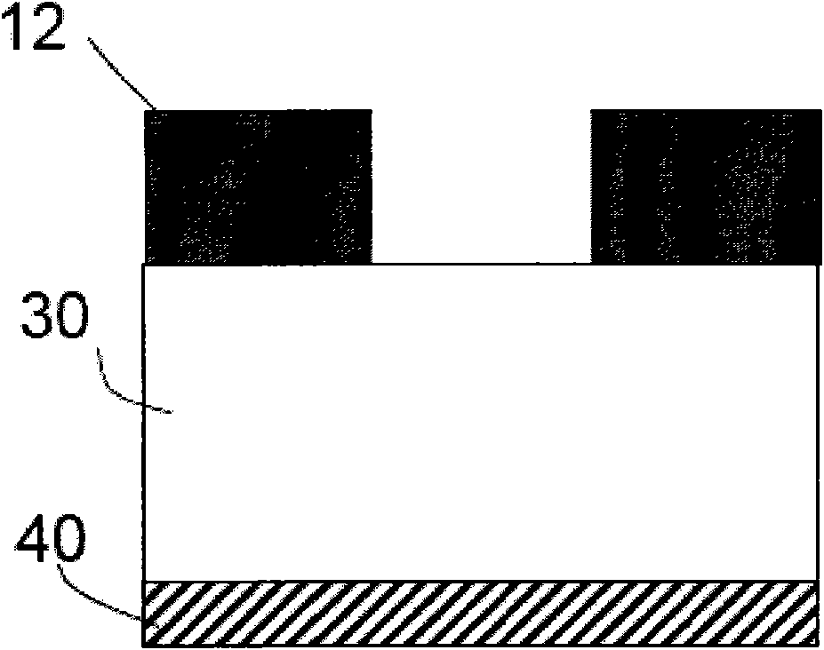
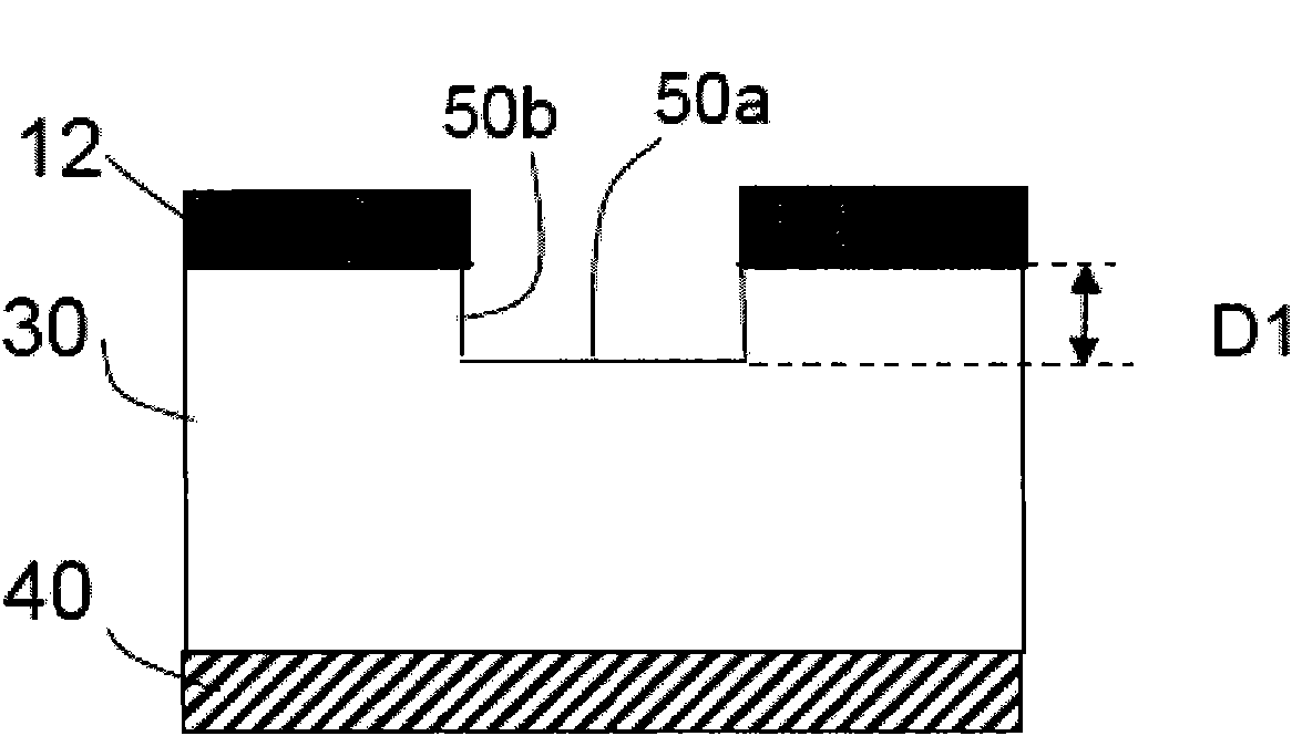
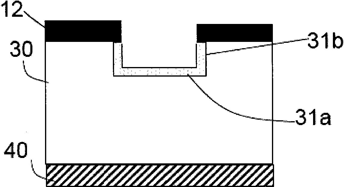
[0019] The invention provides a plasma etching method for an insulating layer containing silicon, which comprises an etching step and a sidewall passivation step (sidewall protection step) carried out independently of each other, and alternately cycles the etching step and the sidewall passivation step during the etching process. Sidewall passivation step until etch reaches target depth. Wherein, in the etching step, an etching gas is provided to etch the silicon-containing insulating material layer under the action of plasma, and etch to a certain depth to expose an etching interface, and the etching interface includes sidewalls; Side wall passivation step, providing a reaction gas containing hydrocarbon components, under the action of plasma, forming a polymer containing hydrocarbon components on the side wall of the etching interface, depositing or adhering to the etching interface side wall surface.
[0020] Using the plasma etching method of the present invention to etch...
PUM
 Abstract
Description
Claims
Application Information