Display element manufacturing method, display element manufacturing apparatus, and display device

A technology for display elements and manufacturing methods, which is applied in the manufacture of discharge tubes/lamps, semiconductor/solid-state device manufacture, electrical components, etc. The effect of high resistance, strong resistance and low cost

Active Publication Date: 2010-08-04
NIKON CORP
View PDF11 Cites 15 Cited by
  • Summary
  • Abstract
  • Description
  • Claims
  • Application Information

AI Technical Summary

Problems solved by technology

[0009] However, although the embodiment disclosed in Patent Document 1 discloses a method for manufacturing a passive liquid crystal cell that can be easily manufactured, it does not relate to the manufacture of a display device having a high-precision drive circuit or a thin film transistor currently in use.
In addition, although the technology of Patent Document 1 uses the droplet coating method to apply conductive ink to form electrodes, there are cases where the conductive ink may not be accurately applied. In this case, a large number of low-reliability display components
In addition, in the case of forming wiring electrodes using the droplet coating method, the droplets coated on the wiring formation surface will spread, so it is difficult to make wiring with a narrow width.
In addition, the applied liquid droplets tend to roll on the wiring formation surface, so it is difficult to form continuous wiring in the desired area.

Method used


Image

  • Display element manufacturing method, display element manufacturing apparatus, and display device
  • Display element manufacturing method, display element manufacturing apparatus, and display device
  • Display element manufacturing method, display element manufacturing apparatus, and display device

Examples


Embodiment 1

[0049] >

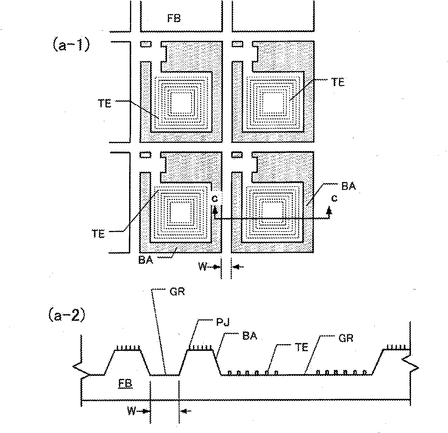
[0050] In the manufacture of an organic EL element, it is necessary to form a substrate including a thin film transistor (TFT) and a pixel electrode. In order to form one or more organic compound layers (light-emitting element layers) including a light-emitting layer with high precision on the pixel electrodes on the substrate, it is necessary to form the barrier ribs BA (banking layer) easily and with high precision in the boundary region of the pixel electrodes. .

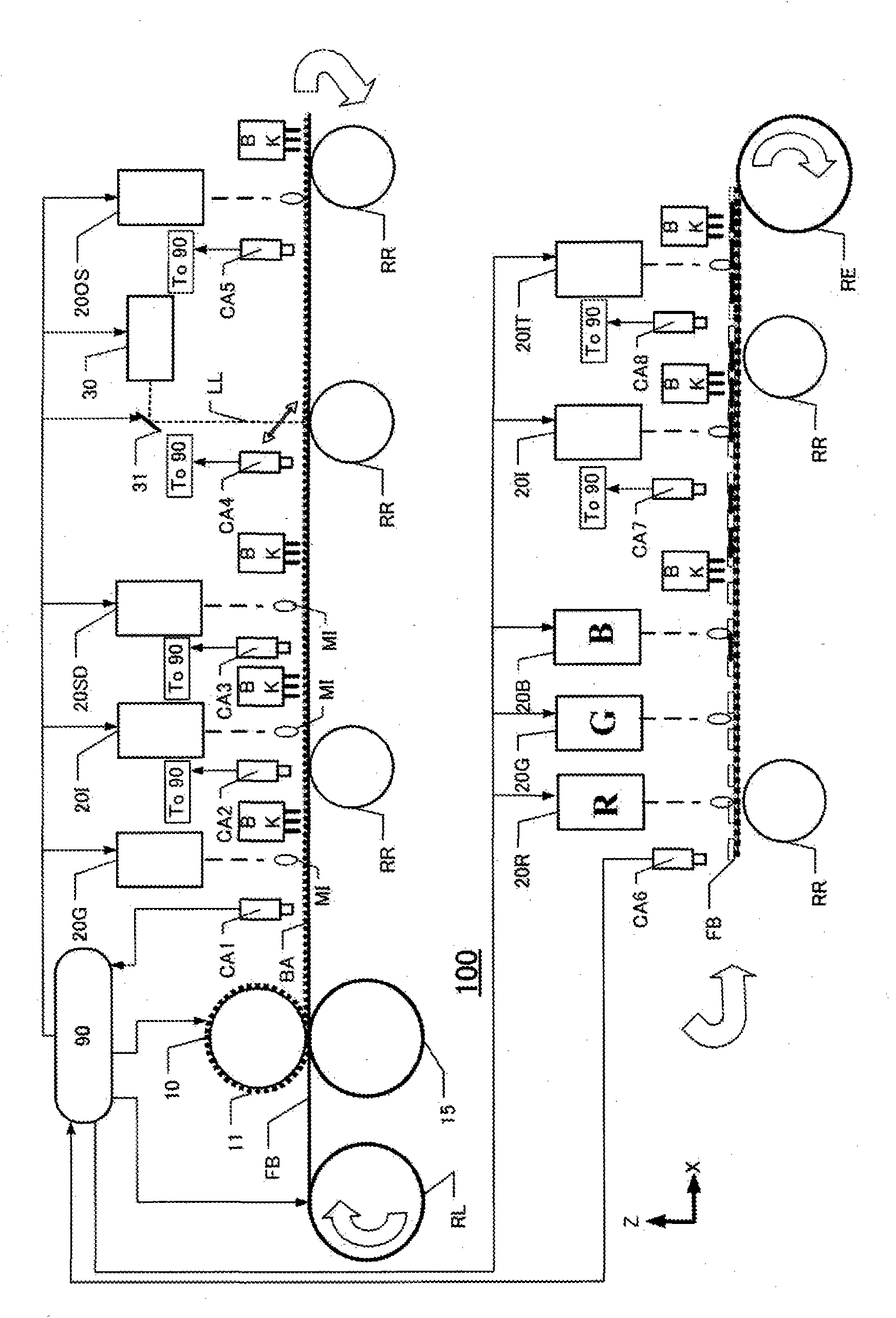
[0051] figure 1 It is a schematic diagram showing the configuration of a manufacturing apparatus 100 for manufacturing organic EL elements including pixel electrodes and light emitting layers on a flexible substrate.

[0052] The manufacturing apparatus 100 for an organic EL element has the supply roll RL for conveying the belt-shaped flexible sheet|seat board|substrate FB wound up into a roll. For example, the length of the sheet substrate FB is, for example, 200 m or more. By rotating the supply ...

Embodiment 2

[0164] >

[0165] Figure 10 It is a schematic diagram showing the structure of a manufacturing apparatus 110 for manufacturing an organic EL element having a pixel electrode, a light emitting layer, etc. on a flexible substrate, and is figure 1 Another example of the manufacturing apparatus 100. However, the same symbols are attached to the same components or devices included in the manufacturing apparatus 100 .

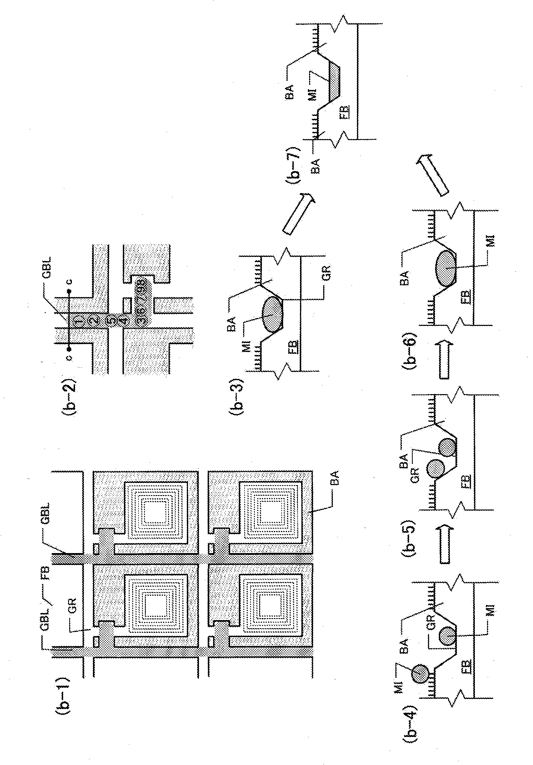
[0166] Figure 10 The fabrication apparatus 110 shown with figure 1 The manufacturing apparatus 100 shown differs in that the partition wall forming process is performed at two locations. The engraving roller 10 forms a partition wall BA for wiring of a thin film transistor, and forms alignment marks AM on both sides of the belt-shaped flexible sheet substrate FB in the Y-axis direction which is the width direction. In addition, in another partition forming step, a printing roll 40 is used.

[0167] The printing roller 40 is formed with a metal mask whose surf...

Embodiment 3

[0172] >

[0173] Next, a manufacturing apparatus and a manufacturing method of a liquid crystal display element will be described. A liquid crystal display element generally consists of a polarizing filter, a sheet substrate FB with a thin film transistor, a liquid crystal layer, a color filter, and a polarizing filter. Among them, for the thin film substrate FB with thin film transistors, it is explained that it can be used in figure 1 The manufacturing device 100 shown in the upper part or in Figure 10 The manufacturing device 110 shown in the upper part is manufactured. In Example 3, the supply of the liquid crystal and the attachment of the color filter CF will be described.

[0174] For a liquid crystal display element, liquid crystal needs to be supplied, and a sealing wall for liquid crystal needs to be formed. Thus, in Figure 10 The printing roller 40 shown in the lower part of the figure is not used to form the partition wall BA for the light-emitting layer in...


PUM

PropertyMeasurementUnit
transmittivityaaaaaaaaaa

Abstract

Provided are a display element manufacturing apparatus for forming a highly reliable drive circuit or thin film transistor on a flexible substrate, a manufacturing method, and a highly reliable display element. A display element (50) comprises a flexible substrate (FB), first and second partitions (BA) formed by pressing the flexible substrate, a lyophobic face (PJ) applied to the surfaces of the first and second partitions, and electrodes (S and P) formed by applying a liquid droplet to a groove between the first and second partitions. Alternatively, a lyophilic face may also be formed on the surface of a groove (GR) between the first and second partitions (BA).

Description

technical field [0001] The present invention relates to flat panel display elements such as an organic electroluminescence (EL) element, a liquid crystal display element, or a field emission display (FED: Electroluminescence Display). Moreover, it also relates to the manufacturing method and manufacturing apparatus of this display element, and relates especially to the display element manufacturing method and manufacturing apparatus which manufacture the drive circuit for driving a display element. Background technique [0002] Display elements such as liquid crystal display elements are currently widely used in various electronic devices due to their small size, thinness, low power consumption, and light weight. A driving circuit or a thin film transistor for driving these display elements is generally manufactured using an exposure device called a stepper. [0003] However, especially with the increase in size of liquid crystal display elements, after reaching the 8th gen...

Claims


Application Information

Patent Timeline
Patent Type & Authority Applications(China)
IPC IPC(8): G09F9/00G02B5/20G02F1/1335H01L51/50H05B33/10H05B33/12H05B33/22H05B33/26H05B33/28G02F1/1333G02F1/1368G09F9/30H01L27/32
CPCH05B33/10H01L51/56G02F1/136286H01L51/0005G02F1/133305H01L51/5206H01L51/0022G02F1/13452G02F1/1368G02F2001/136295G02F1/1303H01J9/148G02F1/136295H10K59/123H10K59/125H10K59/122H10K71/135H10K71/611H10K50/80H10K50/81H10K59/1201H10K2102/311H10K71/00H10K50/00
Inventor 奈良圭浜田智秀
Owner NIKON CORP
Why Eureka
Try Eureka