Solar cell and method for manufacturing the same

A solar cell and battery technology, applied in the field of solar cells, can solve problems such as difficulty in achieving high efficiency yield, inability to absorb equally, and inability to achieve high efficiency, and achieve the effects of preventing degradation, short processing time, and high efficiency

Inactive Publication Date: 2010-08-11
JUSUNG ENG
View PDF0 Cites 4 Cited by
  • Summary
  • Abstract
  • Description
  • Claims
  • Application Information

AI Technical Summary

Problems solved by technology

However, in the case of wafer-type solar cells manufactured using polysilicon having a PN structure, high efficiency cannot be achieved since light in the entire range cannot be equally absorbed
In addition, in the case of thin-film type solar cells having a double-layer PIN structure, it is difficult to achieve high efficiency and increase yield due to long processing time

Method used


Image

  • Solar cell and method for manufacturing the same
  • Solar cell and method for manufacturing the same
  • Solar cell and method for manufacturing the same

Examples


Embodiment Construction

[0034] Reference will now be made in detail to the preferred embodiments of the invention, examples of which are illustrated in the accompanying drawings. Wherever possible, the same reference numbers will be used throughout the drawings to refer to the same or like parts.

[0035] A solar cell and a method of manufacturing the same according to the present invention will be described below with reference to the accompanying drawings.

[0036]

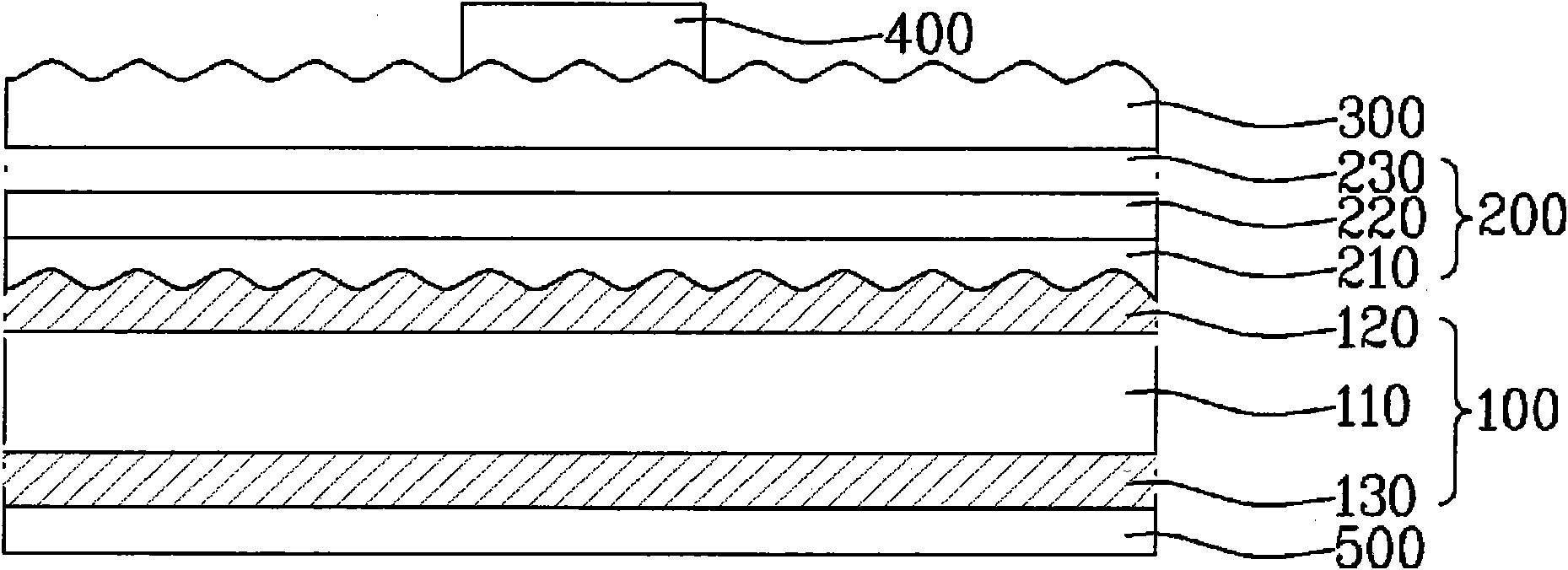
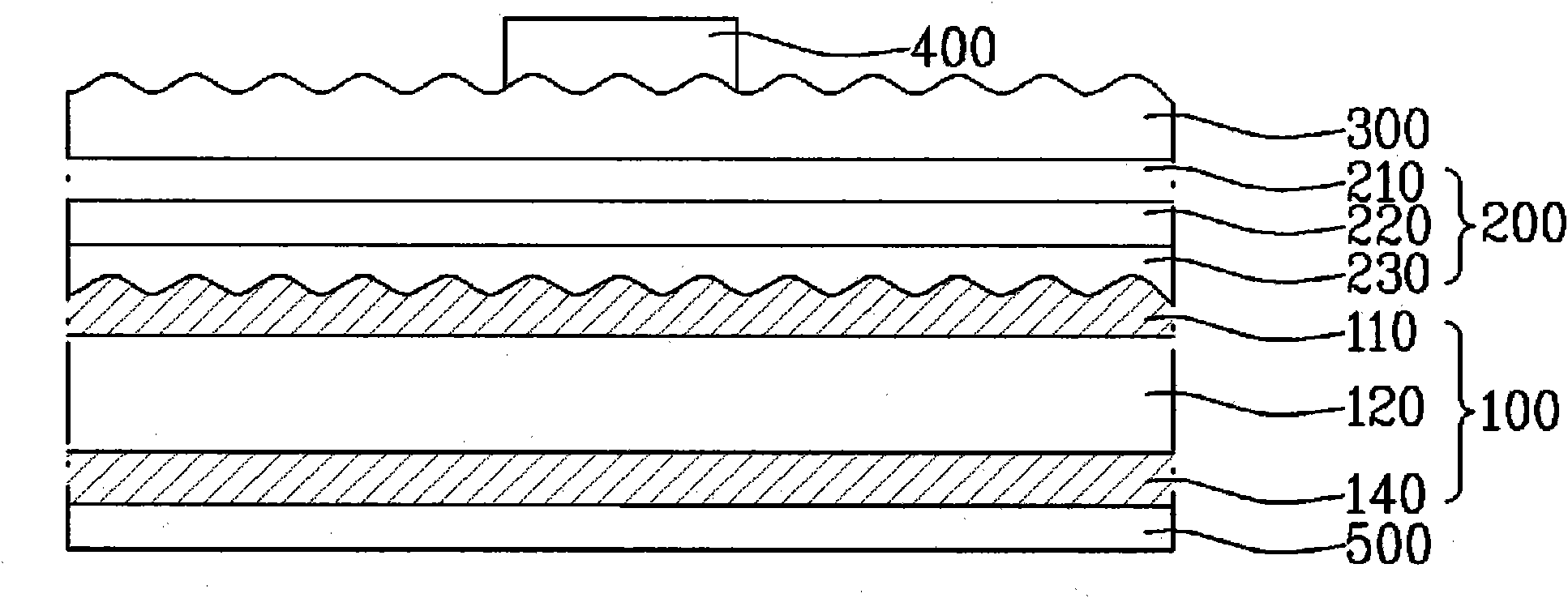
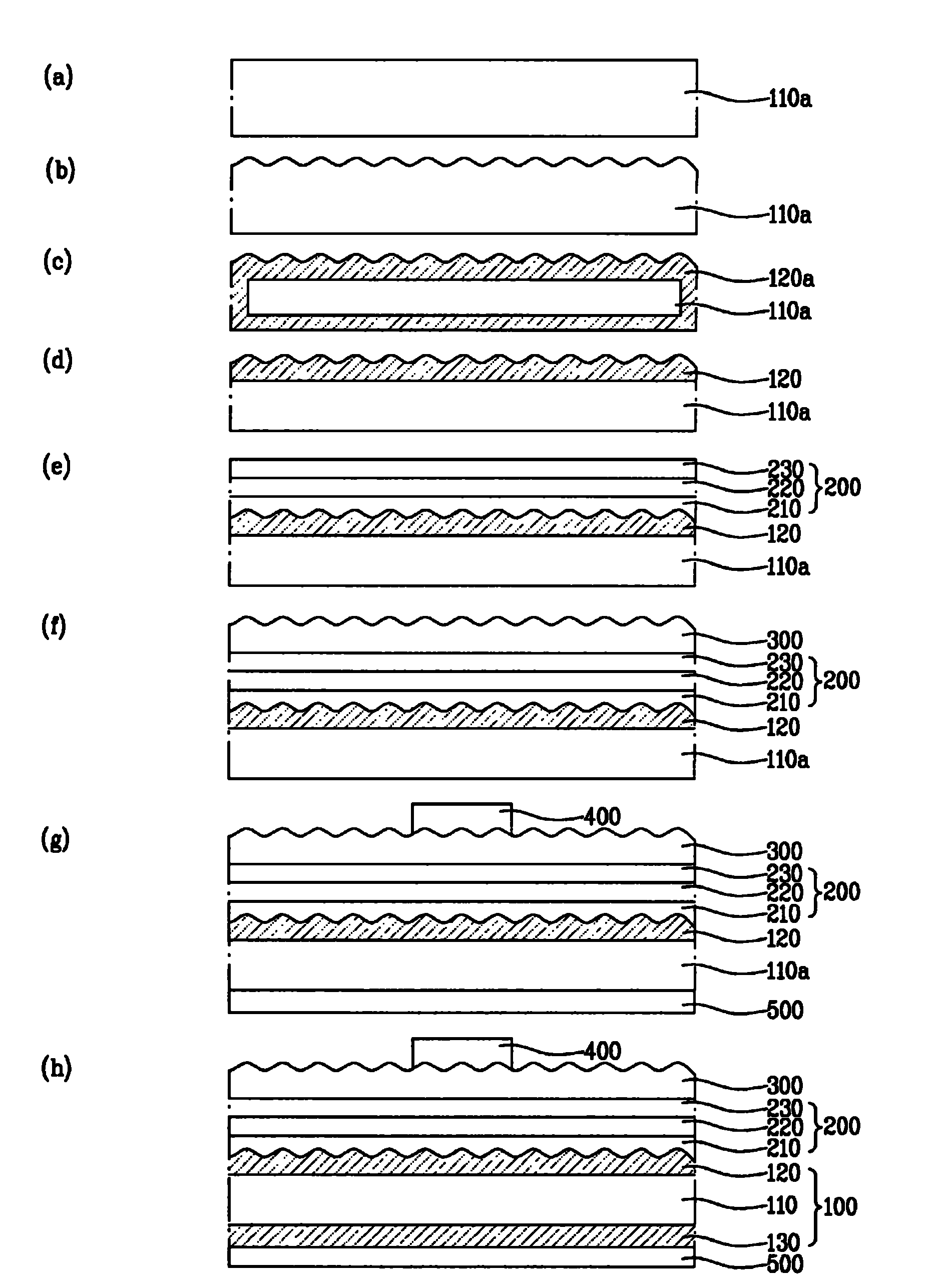
[0037] figure 1 is a cross-sectional view showing a solar cell according to an embodiment of the present invention. Such as figure 1 As shown, the solar cell according to an embodiment of the present invention includes a semiconductor wafer 100 , a thin film semiconductor layer 200 , a transparent conductive layer 300 , a first electrode layer 400 and a second electrode layer 500 .

[0038] The semiconductor wafer 100 forms the first cell of the solar cell, wherein the semiconductor wafer 100 is formed as a PN structure. A semicon...


PUM


Abstract

A solar cell and a method for manufacturing the same is disclosed, wherein the solar cell comprises a first cell comprised of a semiconductor wafer with a PN structure; a second cell comprised of a thin film semiconductor layer with a PIN structure, formed on one surface of the first cell; a first electrode layer formed on one surface of the second cell; and a second electrode layer formed on the other surface of the first cell. Unlike the related art solar cell, the solar cell according to the present invention can absorb the light of long-wavelength range in the first cell, and the light of short-wavelength range in the second cell. As a result, it is possible for the solar cell according to the present invention to absorb the light of all ranges, thereby realizing the high efficiency of 20% or above. Also, the entire process time becomes shortened since there is no requirement for the procedure of forming the silicon thin film for a long period of time.

Description

technical field [0001] The present invention relates to a solar cell, more specifically, to a solar cell manufactured by combining a wafer type solar cell and a thin film type solar cell. Background technique [0002] Solar cells with semiconducting properties convert light energy into electricity. The structure and principle of a solar cell according to the prior art will be briefly explained below. The solar cell is formed in a PN junction structure in which a P (positive) type semiconductor forms a junction with an N (negative) type semiconductor. When sunlight is incident on the solar cell having the PN junction structure, holes (+) and electrons (-) are generated in the semiconductor due to the energy of the sunlight. Under the action of the electric field generated in the PN junction region, the holes (+) drift to the P-type semiconductor, and the electrons (-) drift to the N-type semiconductor, thereby generating electric power, and There is an electric potential. ...

Claims


Application Information

Patent Timeline
Patent Type & Authority Applications(China)
IPC IPC(8): H01L31/042
CPCH01L31/078Y02E10/50H01L31/04H01L31/18
Inventor 洪震金桢植
Owner JUSUNG ENG
Why Eureka
Try Eureka