TFT-LCD (Thin Film Transistor Liquid Crystal Display) array substrate and manufacture method thereof

A manufacturing method and array substrate technology, applied in semiconductor/solid-state device manufacturing, instruments, semiconductor devices, etc., can solve the problems of photoresist deformation in TFT channel area, reduce aperture ratio, increase thin film transistor size, etc., and achieve saving Effects of manufacturing cost, increasing aperture ratio, and increasing brightness

Active Publication Date: 2010-08-18
BOE TECH GRP CO LTD +1
View PDF0 Cites 18 Cited by
  • Summary
  • Abstract
  • Description
  • Claims
  • Application Information

AI Technical Summary

Problems solved by technology

The actual exposure analysis shows that when the ultraviolet light outside the opaque area enters the TFT channel area, the photoresist in the TFT channel area will be too thin, and because the ultraviolet rays entering the TFT channel area from the edge of the opaque area It is not parallel light, and it will also cause deformation of the photoresist in the TFT channel area
Too thin or deformed photoresist will lead to open circuit or short circuit in the TFT channel area during subsequent continuous etching of source and drain metal films and doped semiconductor films, resulting in a decrease in yield
At present, in order to overcome the poor open circuit or short circuit of the TFT channel area, the existing technology adopts the method of increasing the width of the source electrode and the width of the drain electrode, so that the ultraviolet rays outside the opaque area will not enter the TFT channel area, but this method increases The size of the thin film transistor is reduced, the effective light transmission area is reduced, and the aperture ratio is reduced

Method used


Image

  • TFT-LCD (Thin Film Transistor Liquid Crystal Display) array substrate and manufacture method thereof
  • TFT-LCD (Thin Film Transistor Liquid Crystal Display) array substrate and manufacture method thereof
  • TFT-LCD (Thin Film Transistor Liquid Crystal Display) array substrate and manufacture method thereof

Examples


Embodiment Construction

[0062] The technical solutions of the present invention will be described in further detail below with reference to the accompanying drawings and embodiments.

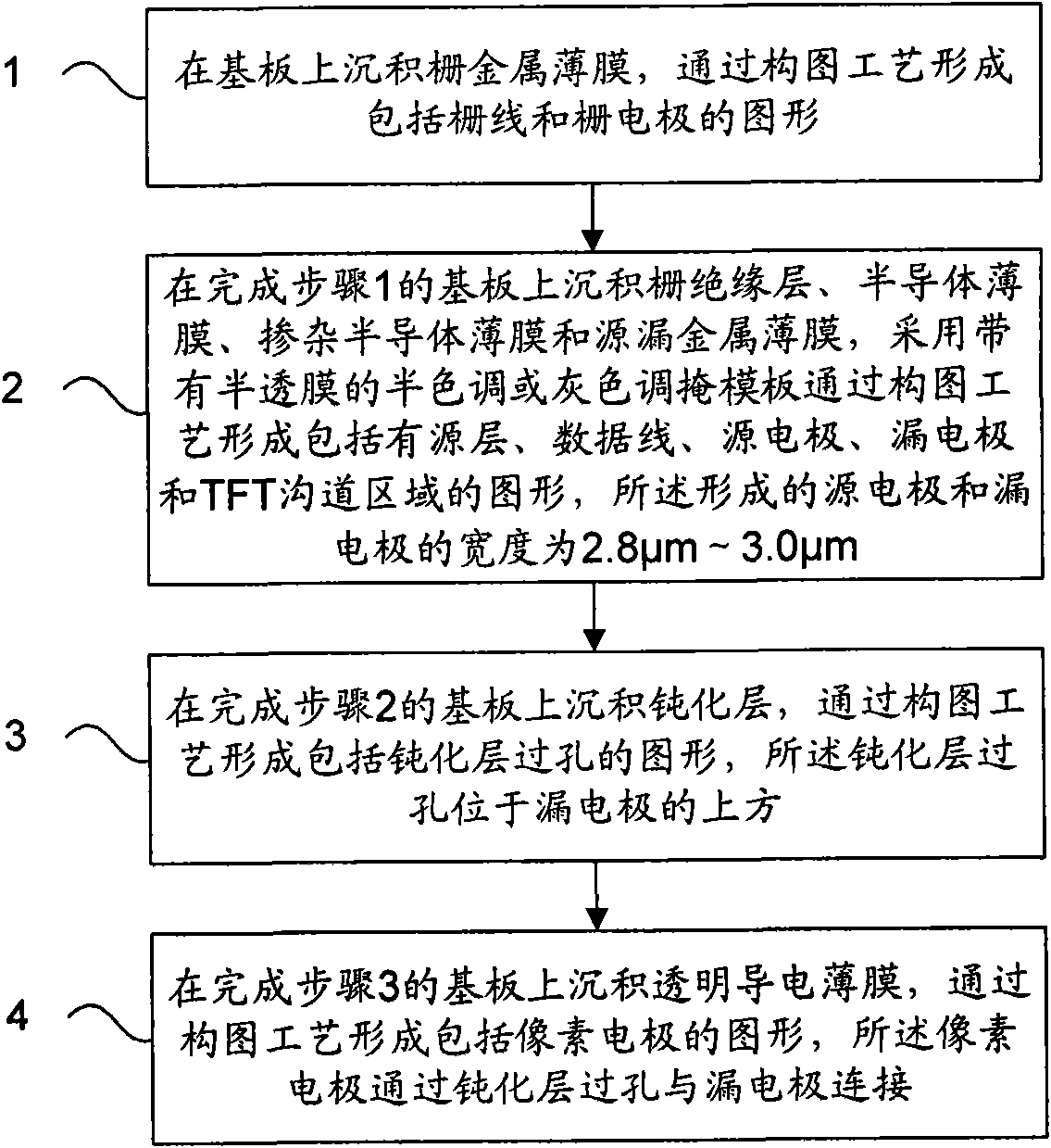
[0063] figure 1 It is a flowchart of the manufacturing method of the TFT-LCD array substrate of the present invention, including:

[0064] Step 1, depositing a gate metal thin film on the substrate, and forming a pattern including a gate line and a gate electrode through a patterning process;

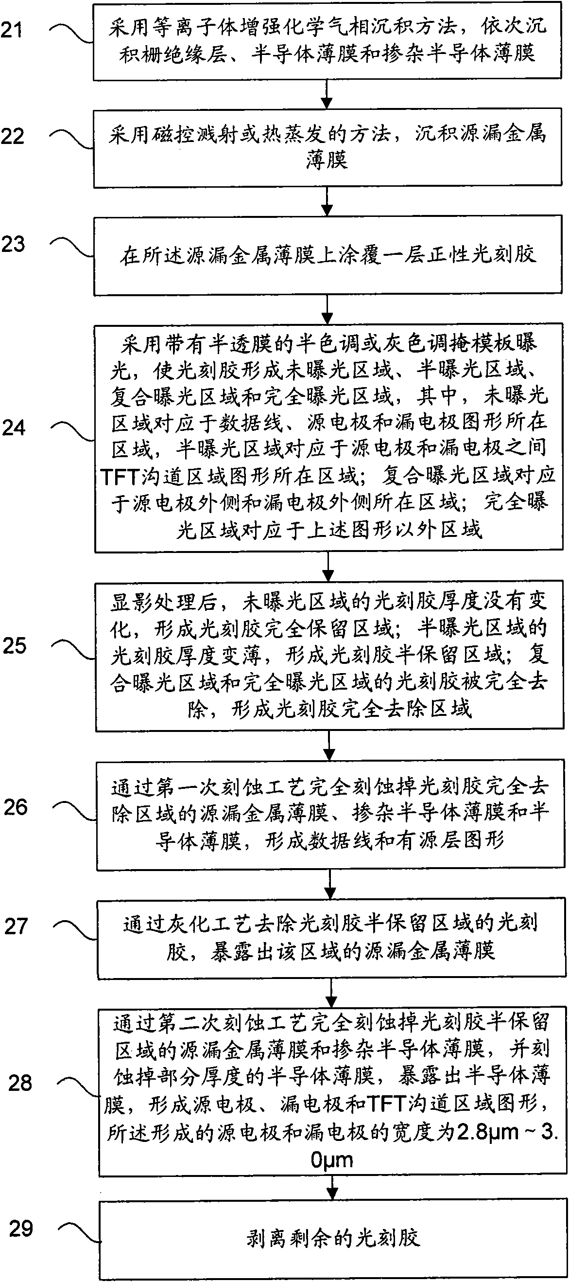
[0065] Step 2. Deposit a gate insulating layer, a semiconductor film, a doped semiconductor film, and a source-drain metal film on the substrate completed in step 1, and use a half-tone or gray-tone mask with a semi-permeable film to form the active layer through a patterning process. 1. Patterns of data lines, source electrodes, drain electrodes and TFT channel regions, the width of the formed source electrodes and drain electrodes is 2.8 μm to 3.0 μm;

[0066] Step 3, depositing a passivation layer on the substrate that comp...


PUM

PropertyMeasurementUnit
widthaaaaaaaaaa
transmittivityaaaaaaaaaa

Abstract

The invention relates to a TFT-LCD (Thin Film Transistor Liquid Crystal Display) array substrate and a manufacture method thereof. The manufacture method comprises the steps of: depositing a grid metal film, forming a grid line and a grid electrode pattern by using a composition process; depositing a grid insulation layer, a semiconductor film, a doped semiconductor film and a source/drain metal film, forming an active layer, a data line, a source electrode, a drain electrode and a TFT channel region pattern by adopting a halftone or gray tone mask template with a semipermeable membrane through a composition process, wherein the widths of the formed source electrode and the formed drain electrode are 2.8-3.0 mu m; depositing a passivation layer, and forming a passivation layer through hole pattern by using the composition process; and depositing a transparent conductive film, forming a pixel electrode pattern by using the composition process, and connecting the pixel electrode with the drain electrode through a passivation layer through hole. The widths of the source electrode and the drain electrode are greatly reduced by adopting the halftone or gray tone mask template with the semipermeable membrane, therefore, the invention improves the aperture opening rate, can increase the brightness and lower the brightness of a backlight board.

Description

technical field [0001] The invention relates to a thin film transistor liquid crystal display structure and a manufacturing method thereof, in particular to a TFT-LCD array substrate and a manufacturing method thereof. Background technique [0002] Thin Film Transistor Liquid Crystal Display (TFT-LCD for short) has the characteristics of small size, low power consumption, and no radiation, and occupies a dominant position in the current flat panel display market. At present, five or four patterning processes are mainly used to manufacture TFT-LCD array substrates in the prior art. The five patterning processes mainly include: patterning of gate lines and gate electrodes, patterning of active layers, patterning of source / drain electrodes, patterning of via holes and patterning of pixel electrodes. The four-step patterning process is based on the five-step patterning process, and uses the half-tone or gray-tone mask technology to combine the active layer patterning and the so...

Claims


Application Information

Patent Timeline
Patent Type & Authority Applications(China)
IPC IPC(8): H01L21/84H01L21/336H01L27/12H01L29/786G02F1/1362
CPCH01L27/1288
Inventor 贠向南金基用鲁成祝曲勇
Owner BOE TECH GRP CO LTD
Why Eureka
Try Eureka