Nano-crystal floating gate nonvolatile memory and manufacturing method thereof

A technology of a non-volatile memory and a manufacturing method, which are applied in the field of nanocrystalline floating gate non-volatile memory and its production, can solve the problems of complex production process, low production efficiency, and the nanocrystalline memory does not have a multi-value storage function.

Inactive Publication Date: 2010-08-18
INST OF MICROELECTRONICS CHINESE ACAD OF SCI
View PDF5 Cites 18 Cited by
  • Summary
  • Abstract
  • Description
  • Claims
  • Application Information

AI Technical Summary

Problems solved by technology

[0013] However, none of the nanocrystalline memories prepared by the above methods has multi-value storage function, and generally there are complicated manufacturing processes, high manufacturing costs, low manufacturing efficiency, or large nanocrystalline particles, or difficult process control during the manufacturing process, or poor feasibility. Disadvantages such as poor compatibility with traditional CMOS processes

Method used


Image

  • Nano-crystal floating gate nonvolatile memory and manufacturing method thereof
  • Nano-crystal floating gate nonvolatile memory and manufacturing method thereof
  • Nano-crystal floating gate nonvolatile memory and manufacturing method thereof

Examples


Embodiment Construction

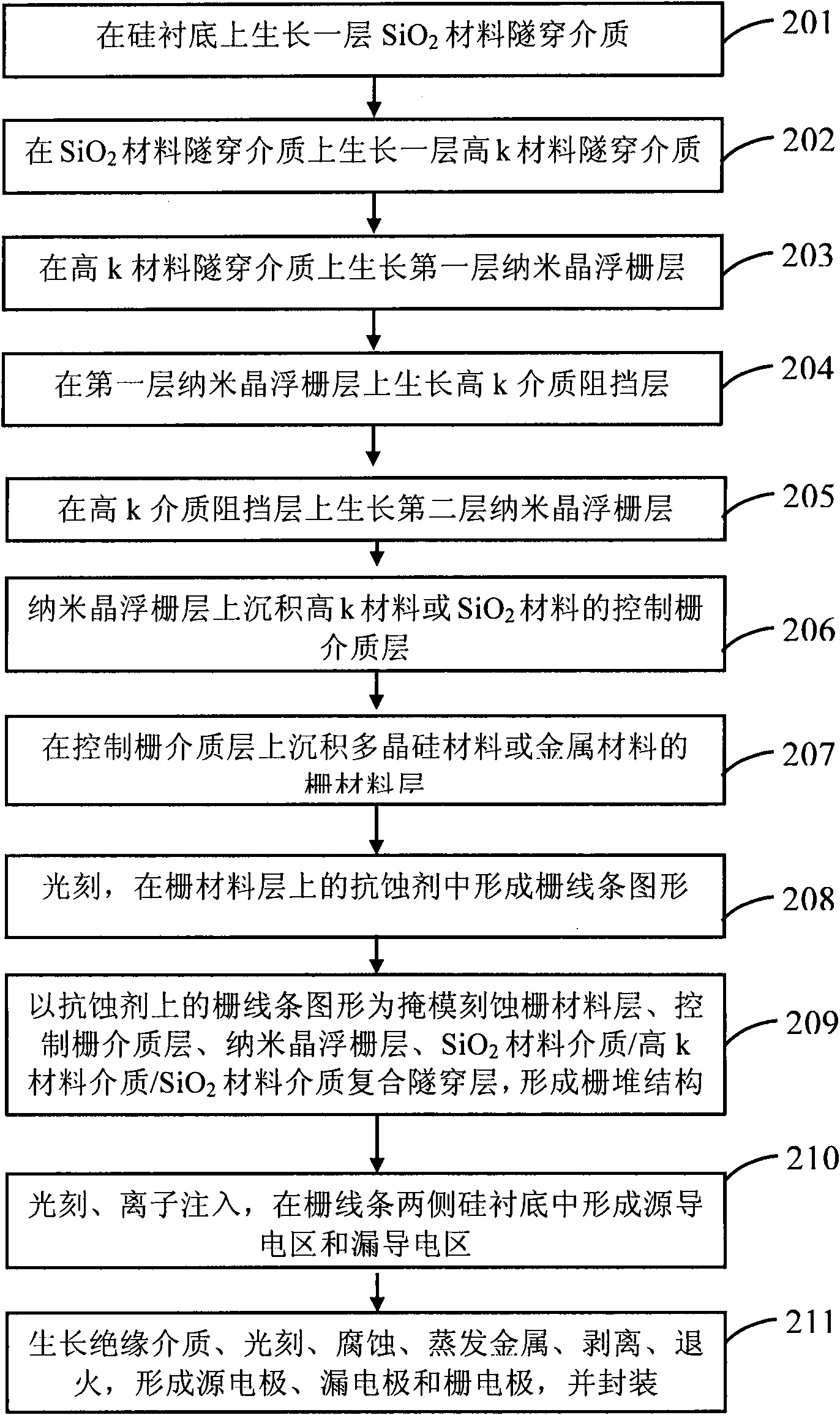
[0095] In order to make the objectives, technical solutions and advantages of the present invention clearer, the present invention will be further described in detail below with reference to specific embodiments and accompanying drawings.

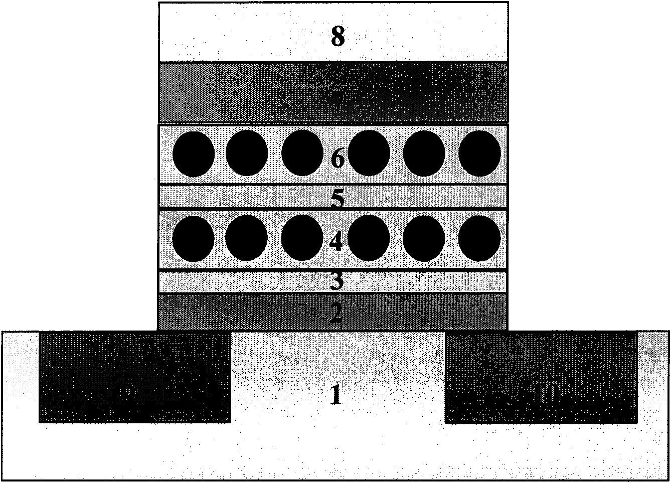
[0096] like figure 1 shown, figure 1 It is a schematic structural diagram of the nanocrystalline floating gate non-volatile memory with multi-value storage function provided by the present invention. The nanocrystalline floating gate nonvolatile memory of the multi-media composite tunneling layer includes: a silicon substrate 1, a silicon substrate on the The heavily doped source and drain regions 9 and 10, and the SiO covering the carrier channel between the source and drain regions 2 Material medium 2 / high-k material medium 3 composite tunneling layer, nanocrystalline floating gate layer 4, high-k material medium 5 used as a double-layer nanocrystalline intercrystalline barrier layer, nanocrystalline floating gate layer 6, on the nanocry...


PUM

PropertyMeasurementUnit
diameteraaaaaaaaaa
thicknessaaaaaaaaaa
thicknessaaaaaaaaaa

Abstract

The invention discloses a nano-crystal floating gate nonvolatile memory with a multi-value storage function and a manufacturing method thereof. The memory comprises a silicon substrate, a source conduction region, a drain conduction region, a composite tunneling layer, a first nano-crystal floating gate layer, a barrier layer medium, a second nano-crystal floating gate layer, a control gate medium layer and a gate material layer, wherein the source conduction region and the drain conduction region are heavily doped on the silicon substrate; the composite tunneling layer is covered on a current carrier channel between the source and drain conduction regions, and consists of an SiO2 material medium and a high-k material medium from the bottom to the top; the first nano-crystal floating gate layer is covered on the composite tunneling layer; the barrier layer medium is covered on the first nano-crystal floating gate layer and used as a barrier layer between double layers of nano-crystals; the second nano-crystal floating gate layer is covered on the barrier layer medium; the control gate medium layer is covered on the second nano-crystal floating gate layer, and consists of a high-k material or an SiO2 material; and the gate material layer is covered on the control gate medium layer. The integration density of the floating gate nonvolatile memory is improved, the storage performance of the memory is comprehensively improved, namely the programming/erasing speed and tolerance and data holding property are improved, and the programming/erasing voltage and the operating power consumption are reduced.

Description

technical field [0001] The invention relates to the technical field of microelectronics, in particular to a nanocrystalline floating gate nonvolatile memory with multi-value storage function and a manufacturing method thereof. Background technique [0002] Floating gate structure memory is a mainstream memory type that is widely used and generally recognized. It is a very important semiconductor component and is widely used in the electronics and computer industries. Due to the choice of its own structure and material, the traditional floating gate structure memory requires the conflicting limitations of fast write / erase operations and long-term high stability storage, and this contradiction is not obvious with the shrinking of technology nodes. improvement, limiting the development of floating gate memory. [0003] As the feature size enters the nanometer level, how to adapt to the development of the process and improve the performance of writing, reading, erasing and reta...

Claims


Application Information

Patent Timeline
Patent Type & Authority Applications(China)
IPC IPC(8): H01L27/115H01L21/8247H01L29/788C23C14/34B82B1/00B82B3/00
Inventor 刘明刘璟王琴胡媛
Owner INST OF MICROELECTRONICS CHINESE ACAD OF SCI
Why Eureka
Try Eureka