
Semiconductor device and method of manufacturing the same

A manufacturing method, semiconductor technology, applied in semiconductor/solid-state device manufacturing, semiconductor devices, semiconductor/solid-state device components, etc., can solve problems such as poor heat dissipation, poorer thermal conductivity than silicon, etc., to improve current capacity and prevent The effect of damage to components and expansion of the heat dissipation area

Inactive Publication Date: 2010-08-18
SANYO ELECTRIC CO LTD +1
View PDF3 Cites 8 Cited by
  • Summary
  • Abstract
  • Description
  • Claims
  • Application Information

AI Technical Summary

Problems solved by technology

Furthermore, since the gate oxide film 39 and the insulating film 41 etc. which are inferior in thermal conductivity to silicon are arranged on the upper surface of the epitaxial layer 33, the surface side of the epitaxial layer 33 becomes a region inferior in heat dissipation.
As a result, in the region indicated by the arrow 43, the surface side of the epitaxial layer 33 is thermally damaged due to the heat generated by the conduction current I2 of the parasitic Tr2.
For example, when an electrostatic destruction test is performed with respect to a structure in which the gate length (W) of the MOS transistor 31 is 1000 μm, the above-mentioned thermal destruction occurs below 1 A with respect to the conduction current I2 (destruction current) of the parasitic Tr2. The machine model (MM) has an ESD tolerance of 200V or less, and the human body model (HBM) has an ESD tolerance of 1000V or less, and it is not a structure that can achieve the desired ESD tolerance

Method used


Image

  • Semiconductor device and method of manufacturing the same
  • Semiconductor device and method of manufacturing the same
  • Semiconductor device and method of manufacturing the same

Examples


Embodiment Construction

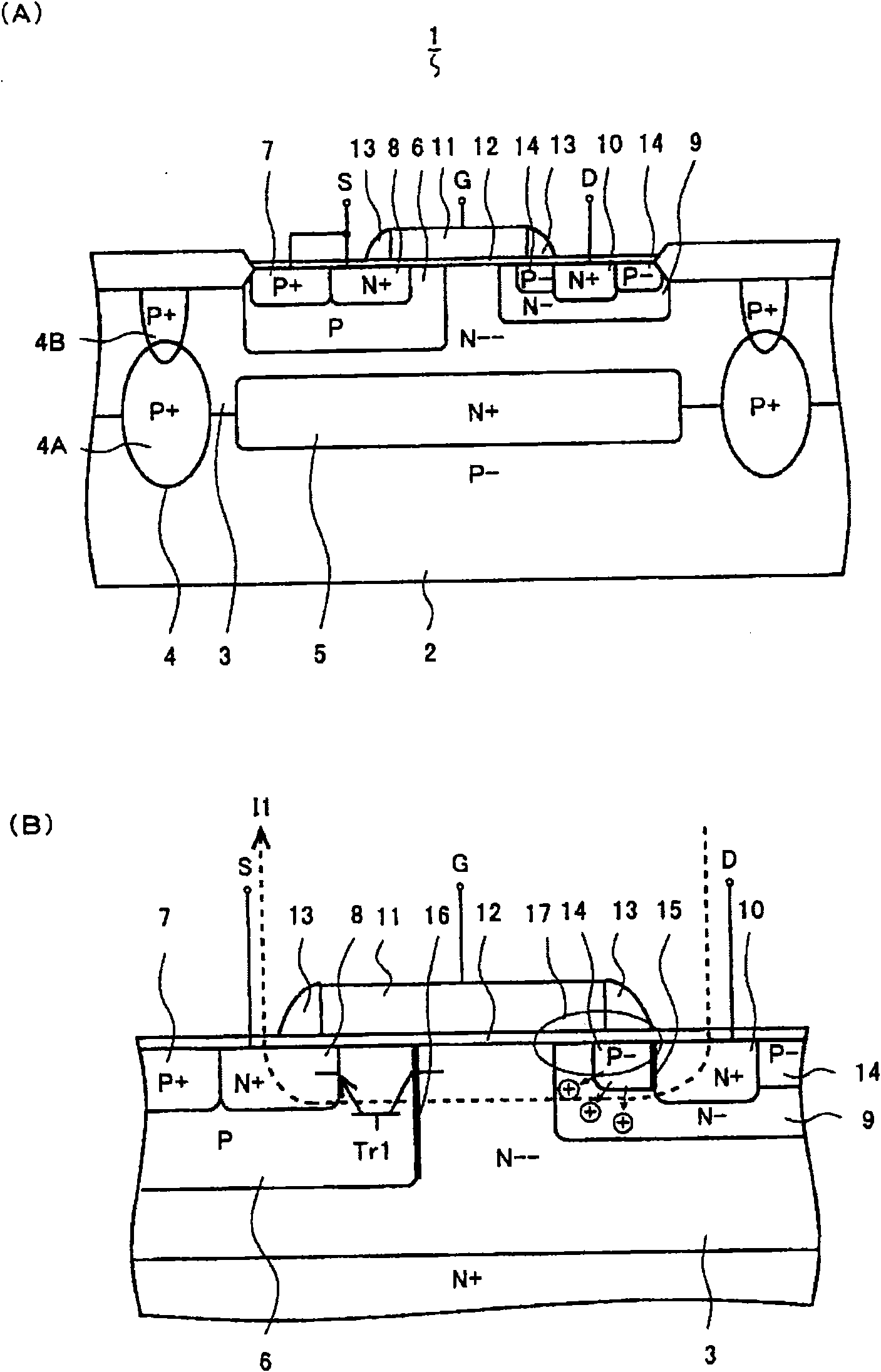
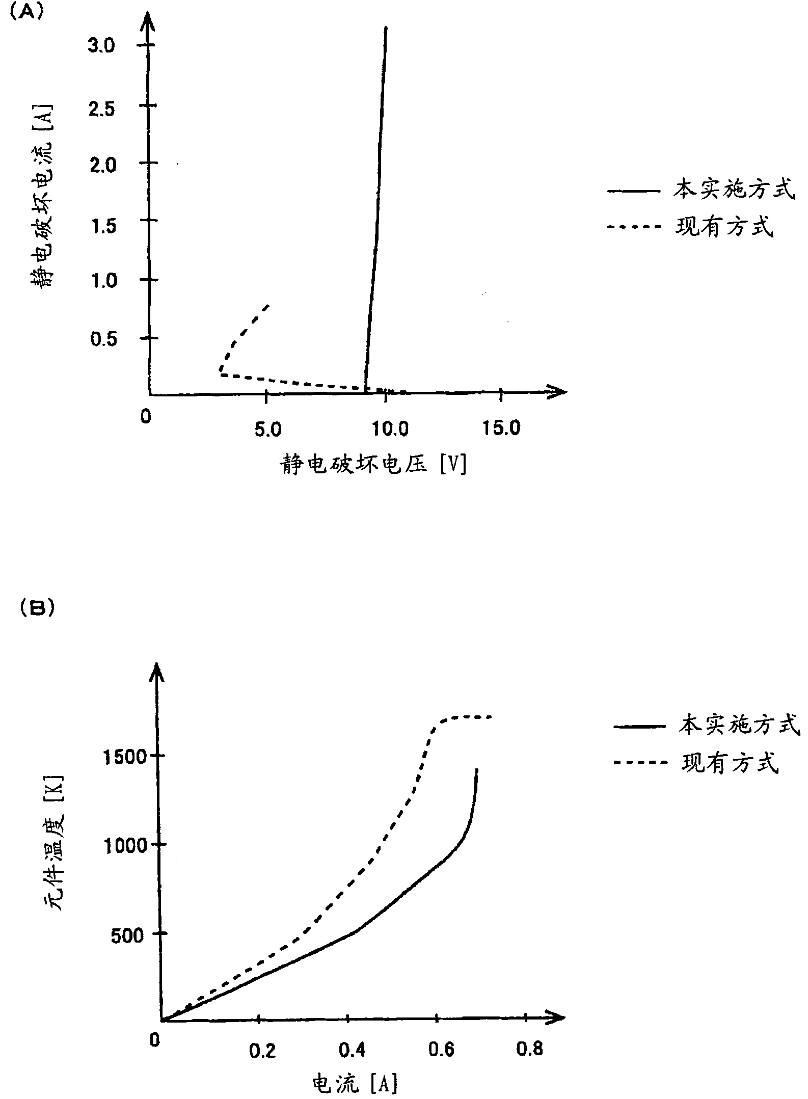
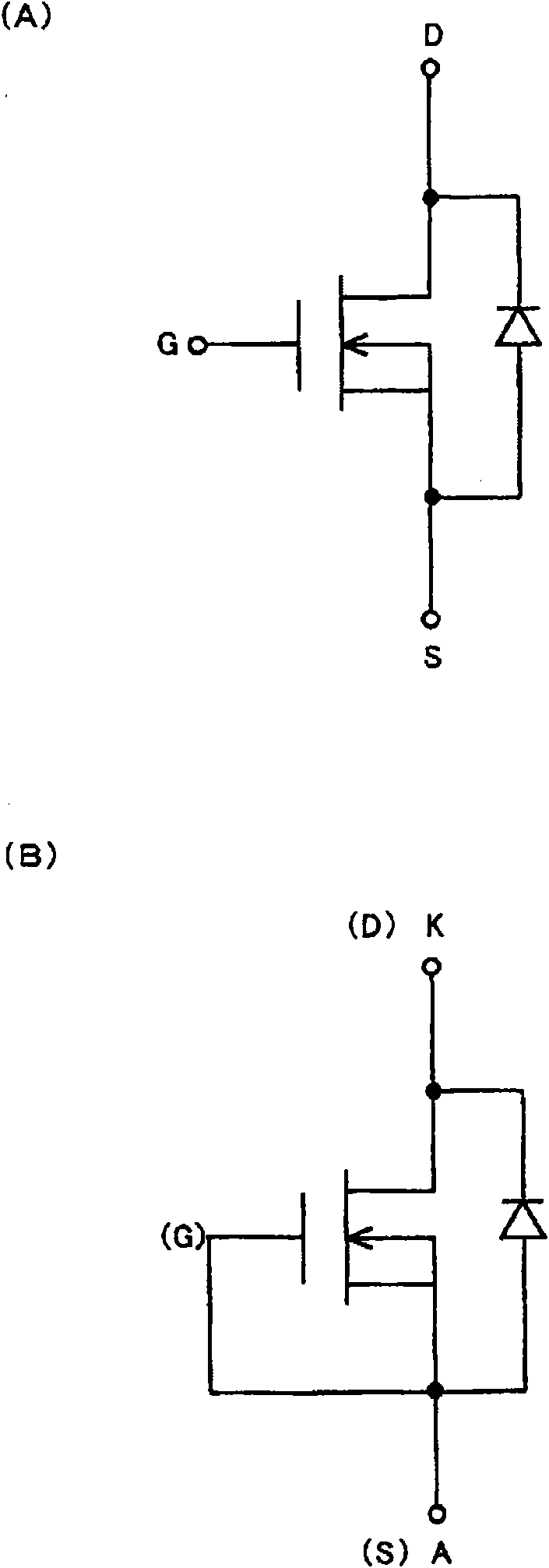
[0026] Below, refer to Figure 1 ~ Figure 3 The semiconductor device according to the first embodiment of the present invention will be described in detail. figure 1 (A) and (B) are cross-sectional views for explaining the MOS transistor of this embodiment. figure 2 (A) and (B) are diagrams for explaining the ESD resistance of the MOS transistor of this embodiment. image 3 (A) and (B) are diagrams for explaining the utilization form of the MOS transistor of this embodiment.

[0027] Such as figure 1 As shown in (A), an N-channel MOS transistor (hereinafter referred to as N-MOS) 1 has a protection structure against overvoltage such as ESD inside the element. As shown in the figure, an N-type epitaxial layer 3 is formed on a P-type single crystal silicon substrate 2 . In addition, in this embodiment, although the case where one epitaxial layer 3 is formed on the substrate 2 is illustrated, it is not limited to this case. For example, it may also be the case where a plur...


PUM


Abstract

In the semiconductor device according to the present invention, a P type diffusion layer and an N type diffusion layer as a drain lead region are formed on an N type diffusion layer as a drain region. The P type diffusion layer is disposed between a source region and the drain region of the MOS transistor. When a positive ESD surge is applied to a drain electrode, causing an on-current of a parasite transistor to flow, this structure allows the on-current of the parasite transistor to take a path flowing through a deep portion of an epitaxial layer. Thus, the heat breakdown of the MOS transistor is prevented.

Description

technical field [0001] The present invention relates to a semiconductor device that prevents destruction due to overvoltage such as Electrostatic Discharge (hereinafter referred to as ESD), and a manufacturing method thereof. Background technique [0002] As an example of a conventional semiconductor device, the following structure of a MOS (Metal Oxide Semiconductor) transistor 31 is known. [0003] Such as Figure 8 As shown, an N-type epitaxial layer 33 is formed on a P-type semiconductor substrate 32 . P-type diffusion layers 34 and 35 serving as back gate regions are formed on the epitaxial layer 33 . An N-type diffusion layer 36 serving as a source region is formed on the P-type diffusion layer 34 . Further, N-type diffusion layers 37 and 38 are formed in the epitaxial layer 33 as drain regions. A gate oxide film 39 , a gate electrode 40 , and an insulating film 41 are formed on the epitaxial layer 33 (for example, refer to Patent Document 1). [0004] Patent Docum...

Claims


Application Information

Patent Timeline
Patent Type & Authority Applications(China)
IPC IPC(8): H01L29/78H01L21/336H01L23/60
CPCH01L29/0873H01L29/0626H01L29/0878H01L29/66689H01L29/7816H01L29/7821H01L29/0696
Inventor 大竹诚治
Owner SANYO ELECTRIC CO LTD
Learn More