

Semiconductor element with improved terminal and manufacturing method thereof
A semiconductor and improved technology, which is applied in the direction of semiconductor/solid-state device manufacturing, semiconductor devices, electrical components, etc., can solve the problem of reducing the integration of cells in the active area of the device, reducing the reliability of the device's withstand voltage, and the limited withstand voltage capability, etc. problems, to achieve the effects of controlling manufacturing costs, improving withstand voltage performance, and increasing breakdown voltage
Active Publication Date: 2010-08-25
WUXI NCE POWER
View PDF5 Cites 13 Cited by
- Summary
- Abstract
- Description
- Claims
- Application Information
AI Technical Summary
Problems solved by technology
When the trench-type power MOS device works in the reverse blocking state, specifically, the device drain applies a voltage drop (the N-type device applies a forward voltage drop, and the P-type device applies a reverse voltage drop), and the gate and the source are connected to zero potential; the reverse blocking state withstand voltage of the trench type power MOS device is shown in Figure 13.a, the conductive polysilicon floating in the trench is induced to a high potential, and the divided voltage The voltage-dividing trench ring corresponding to the active region in the ring bears most of the voltage drop, and the depletion layer will bend upward to the silicon surface along the sidewall of the first trench structure voltage-dividing ring; Specifically, the side wall of the trench corresponding to the side adjacent to the active region in the voltage divider ring, therefore, the width of the depletion layer is much narrower than the original width of the depletion layer parallel to the surface of the semiconductor substrate, resulting in a The potential lines in the depletion layer in the direction of the trench sidewall are too dense, and it is easy to form an excessively strong electric field on the surface of the insulating gate oxide layer on the trench sidewall. Since the thickness of the insulating gate oxide layer is thin, the resistance Limited voltage capability, which reduces the withstand voltage reliability of the device
Secondly, when it is necessary to increase the withstand voltage of the device, it is necessary to increase the number of corresponding voltage divider rings in the terminal protection area; however, when the number of voltage divider rings in the terminal protection area increases, it will also increase the chip area, The Downside of Raising Device Cost
For example, for a 20V trench power MOS device, it is usually necessary to set a voltage divider ring with a trench structure of 2 turns; when the device needs to withstand a voltage of 100V, the voltage divider ring with a trench structure needs to be increased to 10 turns, thus, The area of the terminal protection area will increase by more than 50%, which reduces the integration of cells in the active area of the device and increases the cost of the device
Method used
View moreImage
Smart ImageViewing Examples

Examples
Embodiment Construction
Login to View More PUM
 Abstract
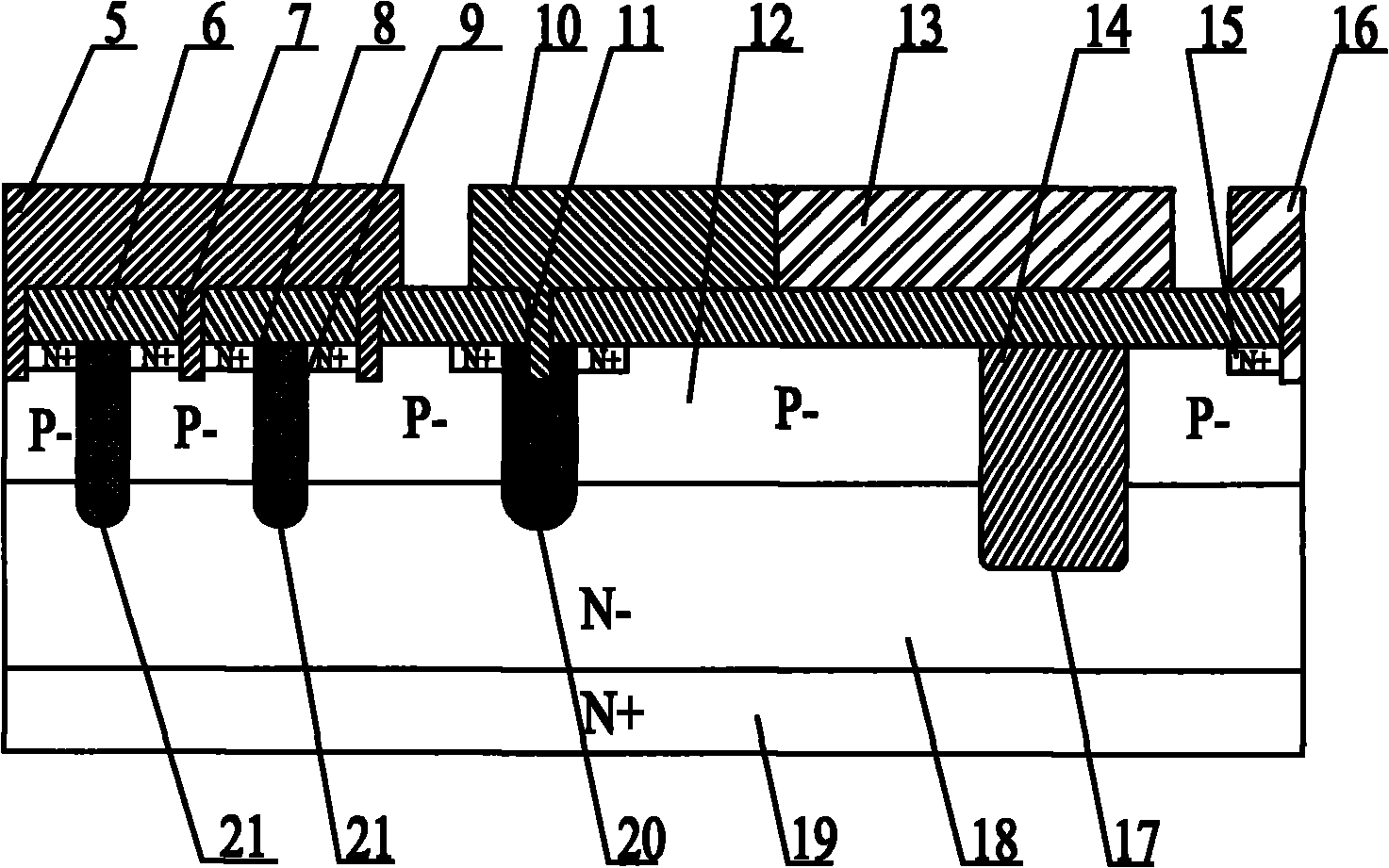
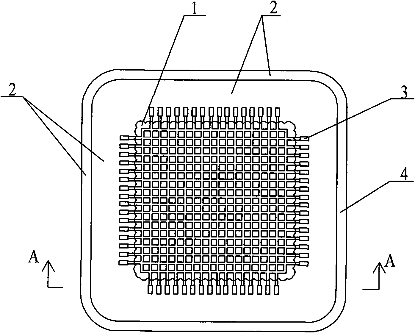
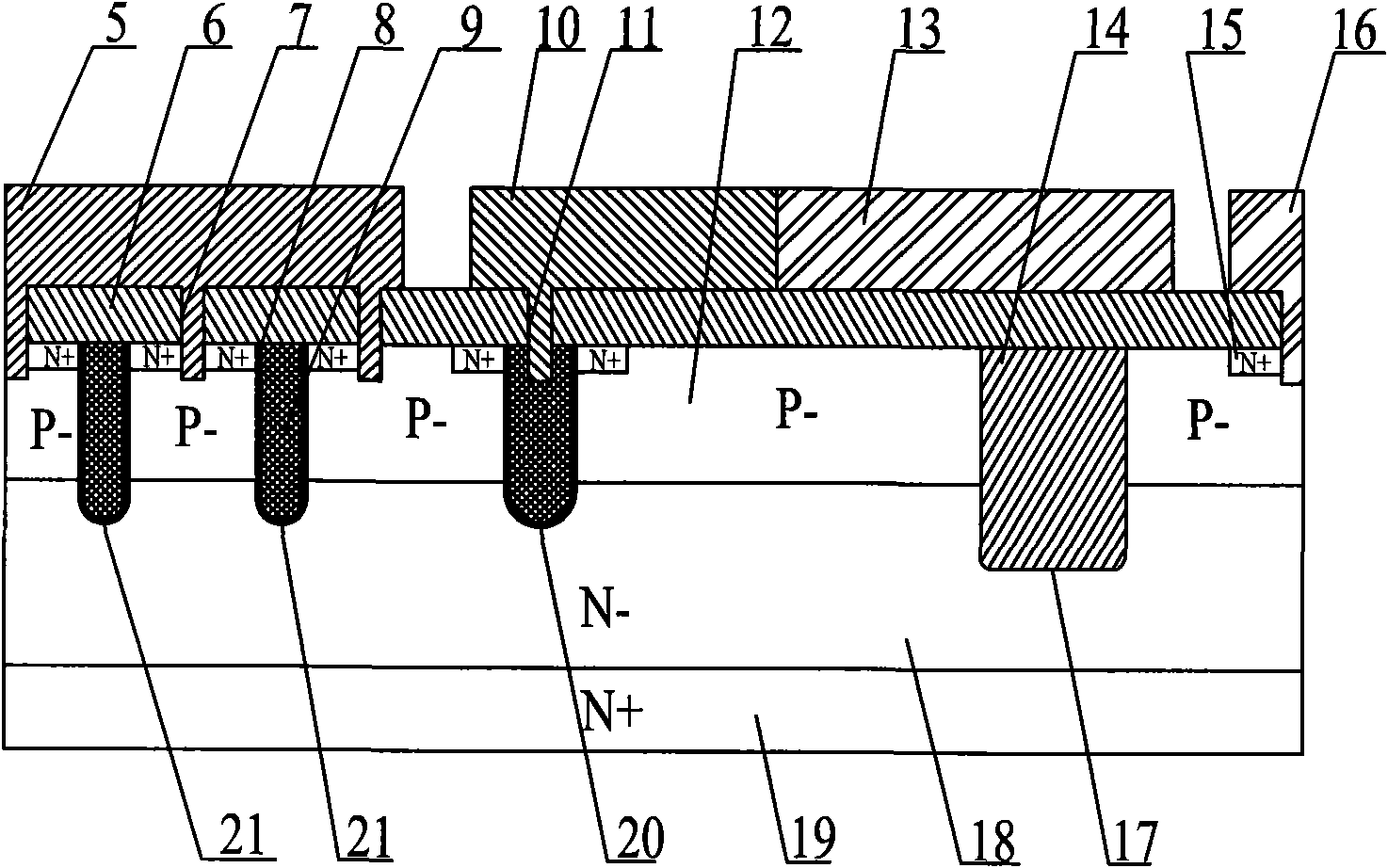
The invention relates to a semiconductor element with an improved terminal and a manufacturing method thereof. A terminal protection area of the element comprises a first flute, wherein a first insulating medium layer is filled in the first flute, and a second insulating medium layer is arranged on the first flute and covers the notch of the first flute and the terminal protective area; a first metal layer covers the second insulating medium layer above the first flute, and is connected with a gate metal or source metal so as to keep a zero electric potential when an MOS element is a reverse blocking state; the first flute is provided with three wire holes corresponding to the side away from an active area, a second metal layer covers the second insulating medium layer and is filled in the three wire holes; and the second metal layer is connected with a first conductive substrate layer by a second conductive layer to form an equipotential. The element has the advantages that: the pressure resistance of the element is ensured; the area of the terminal protection area is controlled; and the manufacturing cost is reduced.
Description
A semiconductor device with an improved terminal and its manufacturing method technical field The invention relates to a semiconductor device and a manufacturing method thereof, in particular to a semiconductor device with an improved terminal and a manufacturing method thereof. Background technique A power semiconductor device generally includes an active area provided for current flow and a terminal protection area provided for protecting the active area. When the power semiconductor device works in the reverse blocking state, the terminal protection area can alleviate the strong electric field at the edge of the active area, improve the withstand voltage of the device, and reduce the leakage current of the device. The structure of the terminal protection area, on the one hand, affects the withstand voltage of the device; on the other hand, it also affects the chip area of the device, that is, it affects the integration of cells in the active area. At present, Chines...
Claims
Login to View More Application Information
Patent Timeline
 Patent Type & AuthorityApplications(China)
IPC IPC(8): H01L29/78H01L21/76H01L21/336
Inventor朱袁正叶鹏丁磊
OwnerWUXI NCE POWER