Structure of light emitting diode chip and manufacture method thereof

A technology of light-emitting diodes and manufacturing methods, which is applied in the direction of electrical components, circuits, semiconductor devices, etc., can solve the problems of low light-emitting efficiency of chips, restricting the development of LEDs, and limited efficiency improvement, so as to improve side wall light-emitting technology and improve light-emitting efficiency , Improve the effect of brightness

Inactive Publication Date: 2010-08-25
EPILIGHT TECH +2
View PDF7 Cites 13 Cited by
  • Summary
  • Abstract
  • Description
  • Claims
  • Application Information

AI Technical Summary

Problems solved by technology

[0004] However, the side of the light-emitting diode chip is smoothed by the blade after scribing, so that the light continues to reflect inside the chip, and most of the light is lost, and the chip's light output efficiency is not high, and the low light output efficiency directly restricts the development of LED
One of the existing methods is to roughen the side of the chip after scribing by etching, so as to improve the light extraction efficiency of the chip, but this method has limited efficiency.

Method used


Image

  • Structure of light emitting diode chip and manufacture method thereof
  • Structure of light emitting diode chip and manufacture method thereof
  • Structure of light emitting diode chip and manufacture method thereof

Examples


Embodiment 1

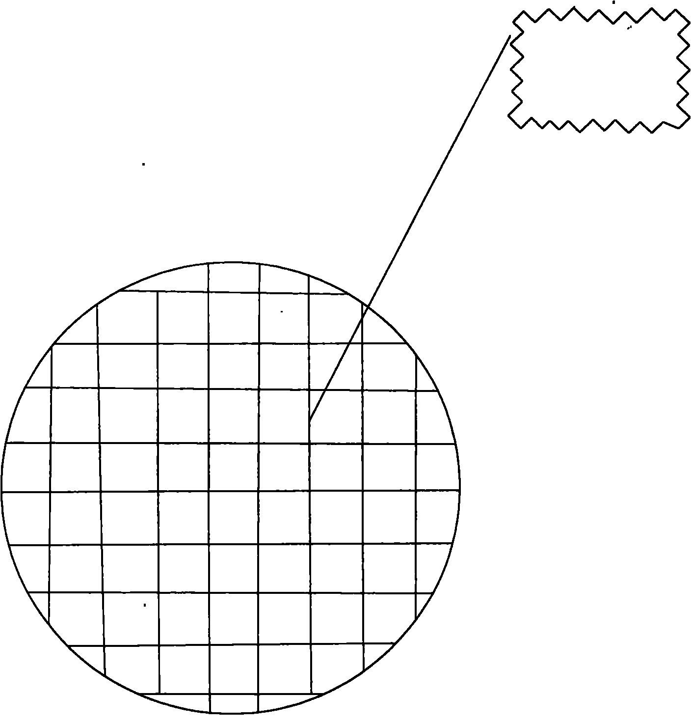
[0039] Step A, first use the laser scribing process to scribe on the growth substrate and form aisles, by adjusting the pulse frequency of the laser source (adjusting the laser frequency, the continuous laser source becomes a discontinuous laser source, which is equivalent to that of the growth substrate. The surface is dotted, the frequency of a normal dicing machine is 100KHZ, and the laser frequency of the present invention is below 30KHZ. The edge of the cross section (section perpendicular to the epitaxial growth direction) of the growth substrate is divided into zigzag or wave shape.

[0040] The aisle directly divides the surface of the growth substrate into small areas identical to the final chip size, defines the chip size (defining the growth substrate), and forms an aisle depth of 15-50 microns; the preferred range of the general aisle depth is 15- 20 microns, and the preferred aisle depth is around 20 microns. The growth substrate may be a Si growth substrate, a Si...

Embodiment 2

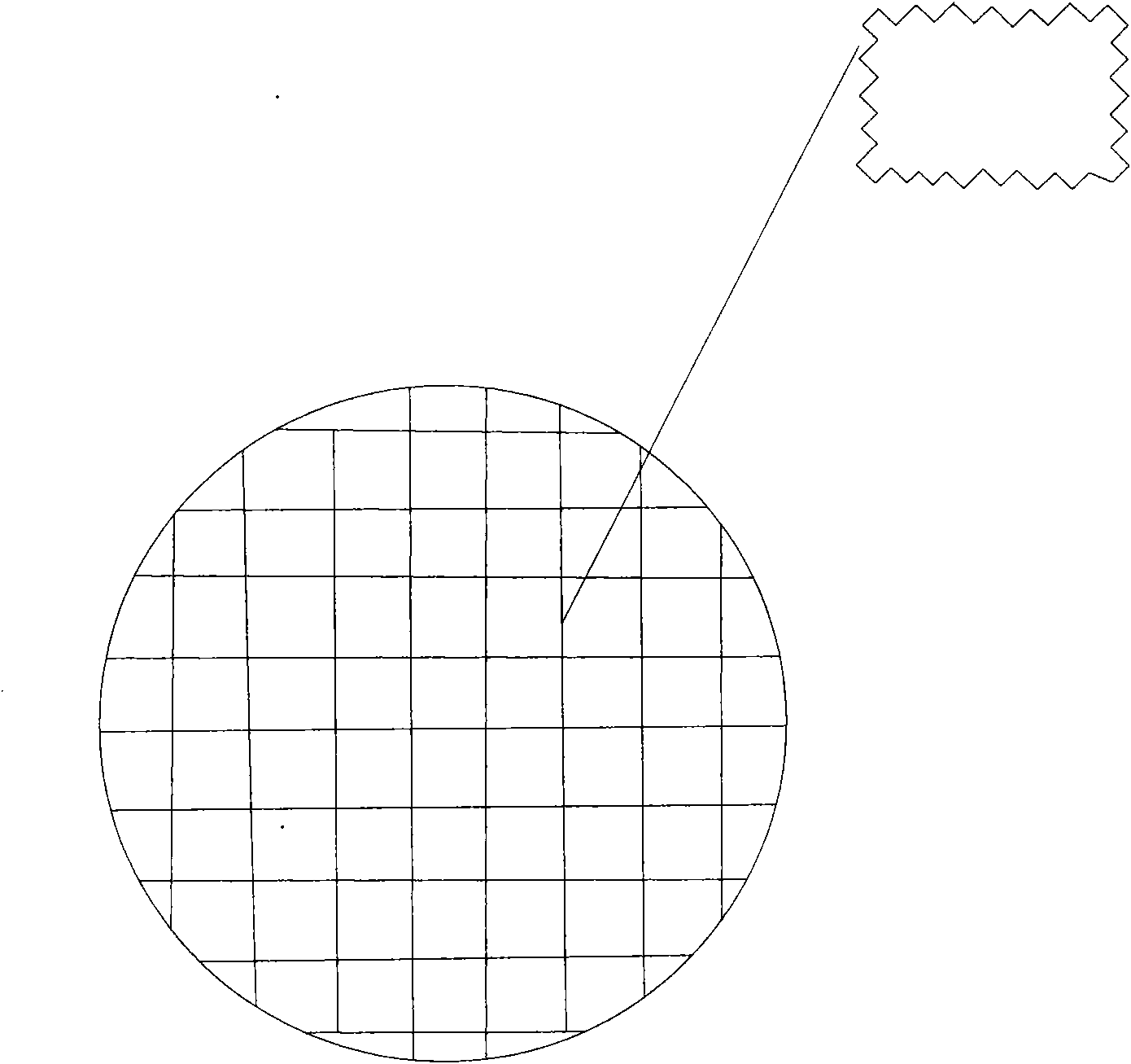
[0049] Step A, first growing a semiconductor epitaxial layer on a growth substrate. Patterns can be formed on the growth substrate by using techniques such as photolithography and dry etching technology or wet etching technology to make a patterned growth substrate. An N-type semiconductor layer, an active layer, and a P-type semiconductor layer are epitaxially grown sequentially on the patterned growth substrate. The N-type semiconductor layer is preferably an N-type GaN layer, the P-type semiconductor layer is preferably a P-type GaN layer, and the active layer is preferably a GaN-based quantum well layer.

[0050] Step B, by adjusting the pulse frequency of the laser source (adjust the laser frequency so that the continuous laser source becomes an intermittent laser source, which is equivalent to dotting on the surface of the growth substrate), the pulse frequency of the laser source is 20KHZ, and the semiconductor epitaxy The edges of the cross-section (section perpendicu...

Embodiment 3

[0055] The difference between the third embodiment and the second embodiment is only that the semiconductor epitaxial layer is adjusted by adjusting the pulse frequency of the laser source (adjusting the laser frequency to make the continuous laser source become a discontinuous laser source, which is equivalent to dotting the surface of the growth substrate). And the edge of the cross section of the growth substrate (the cross section perpendicular to the epitaxial growth direction) is drawn into a zigzag or wave shape, and the pulse frequency of the laser source is 25KHZ. That is, the sidewalls of the semiconductor epitaxial layer and the growth substrate are both wavy.

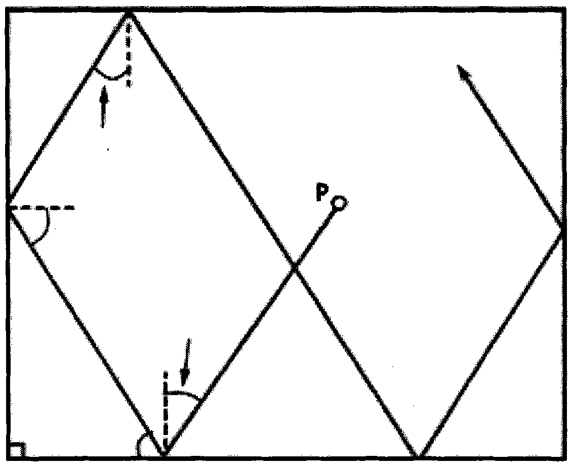
[0056] Please refer to Fig. 2, since the sidewall of a conventional chip is vertical, when the radiated photon P is at an incident angle θ 1 Arriving at the first wall w1, after reflection, it will be at the incident angle θ 2 Reaching the second wall w2 (i.e. the side wall), after reflection again, it will...


PUM


Abstract

The invention relates to a structure of a light emitting diode chip and a manufacture method thereof. The structure comprises a growth substrate and a semiconductor epitaxial layer, wherein the semiconductor epitaxial layer is positioned on the growth substrate, the edges of the cross sections of either the growth substrate or the semiconductor epitaxial layer or the edges of the cross sections of both the growth substrate and the semiconductor epitaxial layer are in a sawtooth shape or a wave shape. The structure enhances the area of the side wall of the chip, the light outlet angle of the chip is regulation, and the brightness of the chip is obviously improved. Through the side wall micro structure technology, the invention improves the integral light outlet efficiency of the chip, and the light outlet efficiency is improved by more than 25 percent.

Description

technical field [0001] The invention relates to the field of light-emitting diode manufacturing, in particular to the structure of a light-emitting diode chip capable of improving the light-emitting efficiency of the chip and its manufacturing method. Background technique [0002] Light-emitting diodes have the advantages of small size, high efficiency and long life, and are widely used in traffic indication, outdoor full-color display and other fields. In particular, the use of high-power light-emitting diodes may realize semiconductor solid-state lighting, which has caused a revolution in the history of human lighting, and has gradually become a research hotspot in the field of electronics. [0003] The traditional chip manufacturing process is to prepare hundreds or even thousands of chips on a growth substrate at the same time, with a certain distance between each chip. After preparing these chips, they are separated by dicing and cutting, and finally A light-emitting d...

Claims


Application Information

Patent Timeline
Patent Type & Authority Applications(China)
IPC IPC(8): H01L33/20
Inventor 张楠周健华郝茂盛叶青潘尧波朱广敏齐胜利杨卫桥
Owner EPILIGHT TECH
Why Eureka
Try Eureka