TFT-LCD (Thin Film Transistor Liquid Crystal Display) array substrate and manufacture method thereof

An array substrate and substrate technology, applied in the structure of thin film transistor liquid crystal display and its manufacturing field, can solve the problem of small storage capacitance, achieve the effect of improving the interface, reducing the distance, and increasing the storage capacitance per unit area

Active Publication Date: 2010-09-01
BOE TECH GRP CO LTD +1
View PDF0 Cites 16 Cited by
  • Summary
  • Abstract
  • Description
  • Claims
  • Application Information

AI Technical Summary

Problems solved by technology

But no matter what type, the prior art uses a gate metal film as one electrode plate of the storage capacitor, and a gate insulating layer and a passivation layer are interposed between the pixel electrode as the other electrode plate of the storage capacitor. Thickness is The thickness of the passivation layer is It can be seen from the calculation formula of the storage capacitor that the size of the storage capacitor per unit area is inversely proportional to the distance between the two electrode plates. Since the distance between the two electrode plates of the storage capacitor in the existing TFT-LCD array substrate is relatively large, the unit area The storage capacitor is relatively small

Method used


Image

  • TFT-LCD (Thin Film Transistor Liquid Crystal Display) array substrate and manufacture method thereof
  • TFT-LCD (Thin Film Transistor Liquid Crystal Display) array substrate and manufacture method thereof
  • TFT-LCD (Thin Film Transistor Liquid Crystal Display) array substrate and manufacture method thereof

Examples


preparation example Construction

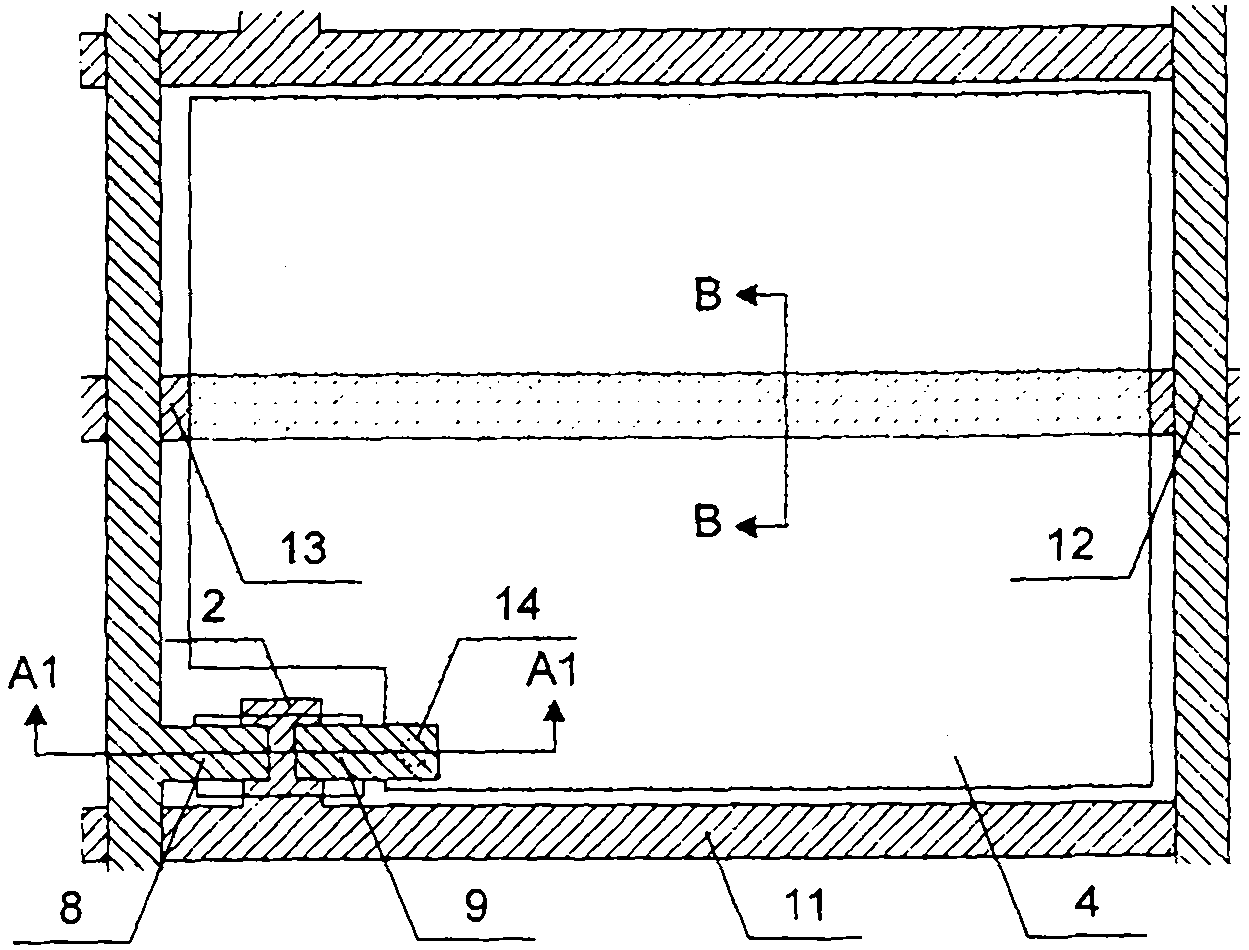
[0070] The preparation process of the TFT-LCD array substrate of this embodiment is basically the same as that of the aforementioned first embodiment. The formed pixel electrodes 4 cover part of the gate lines 11 , and the similarities will not be repeated here.

[0071] In practical applications, the present invention can also form a storage capacitor structure in which part of the storage capacitor is on the gate line and the other part is on the common electrode line, that is, combining the aforementioned first embodiment and the second embodiment to form a combined structure. The common electrode lines are arranged in the area, and on the other hand, the pixel electrodes cover part of the gate lines.

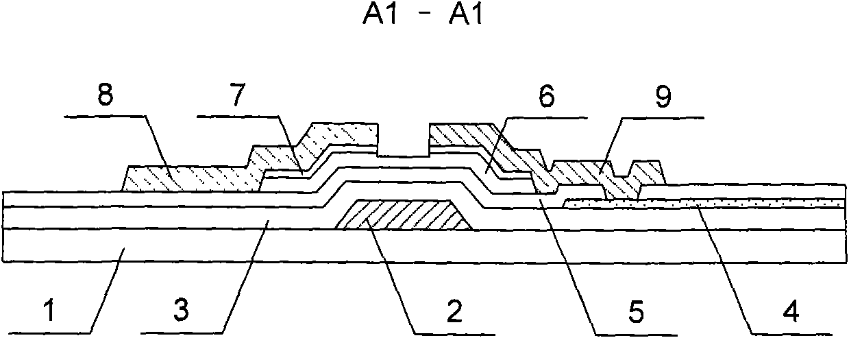
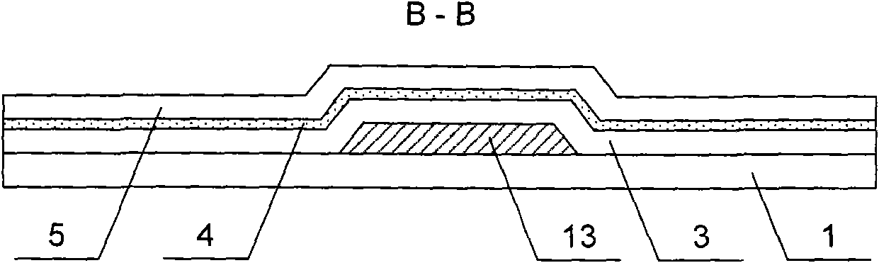
[0072] The above-mentioned embodiments of the present invention provide a TFT-LCD array substrate. By arranging two insulating layers and disposing the pixel electrode between the two insulating layers, when the pixel electrode forms a storage capacitor with the common elect...


PUM


Abstract

The invention relates to a TFT-LCD (Thin Film Transistor Liquid Crystal Display) array substrate and a manufacture method thereof. The array substrate comprises a grid line and a data line which are formed on the substrate, wherein a pixel electrode and a thin film transistor are formed in a pixel region limited by the grid line and the data line; a first insulating layer and a second insulating layer are formed between the grid line and the data line; and the pixel electrode is arranged between the first insulating layer and the second insulating layer. In the invention, through arranging the two insulating layers and arranging the pixel electrode between the two insulating layers, when the pixel electrode forms a memory capacitor with a common electrode line or the grid line, the distance between two electrode plates of the memory capacitor is only equal to the thickness of the first insulating layer, thus the distance between the two electrode plates of the memory capacitor is greatly reduced, and the memory capacitor of a unit area is greatly improved. Furthermore, because the structure of the two insulating layers is adopted, an interface formed between the insulating layers and a semiconductor layer can be improved so as to improve the characteristics of the TFT.

Description

technical field [0001] The invention relates to a thin film transistor liquid crystal display structure and a manufacturing method thereof, in particular to a TFT-LCD array substrate and a manufacturing method thereof. Background technique [0002] Thin Film Transistor Liquid Crystal Display (TFT-LCD for short) has the characteristics of small size, low power consumption, and no radiation, and occupies a dominant position in the current flat panel display market. [0003] TFT-LCD is mainly composed of an array substrate and a color filter substrate in a box, wherein thin-film transistors and pixel electrodes arranged in a matrix are formed on the array substrate, and each pixel electrode is controlled by a thin-film transistor. When the thin film transistor is turned on, the pixel electrode is charged during the turn-on time, and after the charging is completed, the voltage of the pixel electrode will be maintained until recharging in the next scan. Generally speaking, the ...

Claims


Application Information

Patent Timeline
Patent Type & Authority Applications(China)
IPC IPC(8): G02F1/1362H01L27/12H01L21/84H01L21/02
CPCH01L27/1214H01L33/08H01L27/1288H01L27/124H01L27/1248G02F1/1343G02F1/136286
Inventor 刘翔林承武陈旭谢振宇
Owner BOE TECH GRP CO LTD
Why Eureka
Try Eureka