Optical waveguide sensor and preparation methods thereof

A manufacturing method and optical waveguide technology, applied to the coupling of optical waveguides, the use of optical devices to transmit sensing components, instruments, etc., can solve the problems of difficult resolution, low efficiency, and high cost of high-temperature optical fiber sensors, and achieve low production costs. high efficiency effect

Inactive Publication Date: 2010-09-15
无锡光芯科技有限公司
View PDF7 Cites 15 Cited by
  • Summary
  • Abstract
  • Description
  • Claims
  • Application Information

AI Technical Summary

Problems solved by technology

[0010] In order to solve the problem that the multiple peaks produced by Bragg gratings on the multimode sapphire optical fiber are not easy to distinguish, and the high cost...

Method used


Image

  • Optical waveguide sensor and preparation methods thereof
  • Optical waveguide sensor and preparation methods thereof
  • Optical waveguide sensor and preparation methods thereof

Examples


Embodiment 1

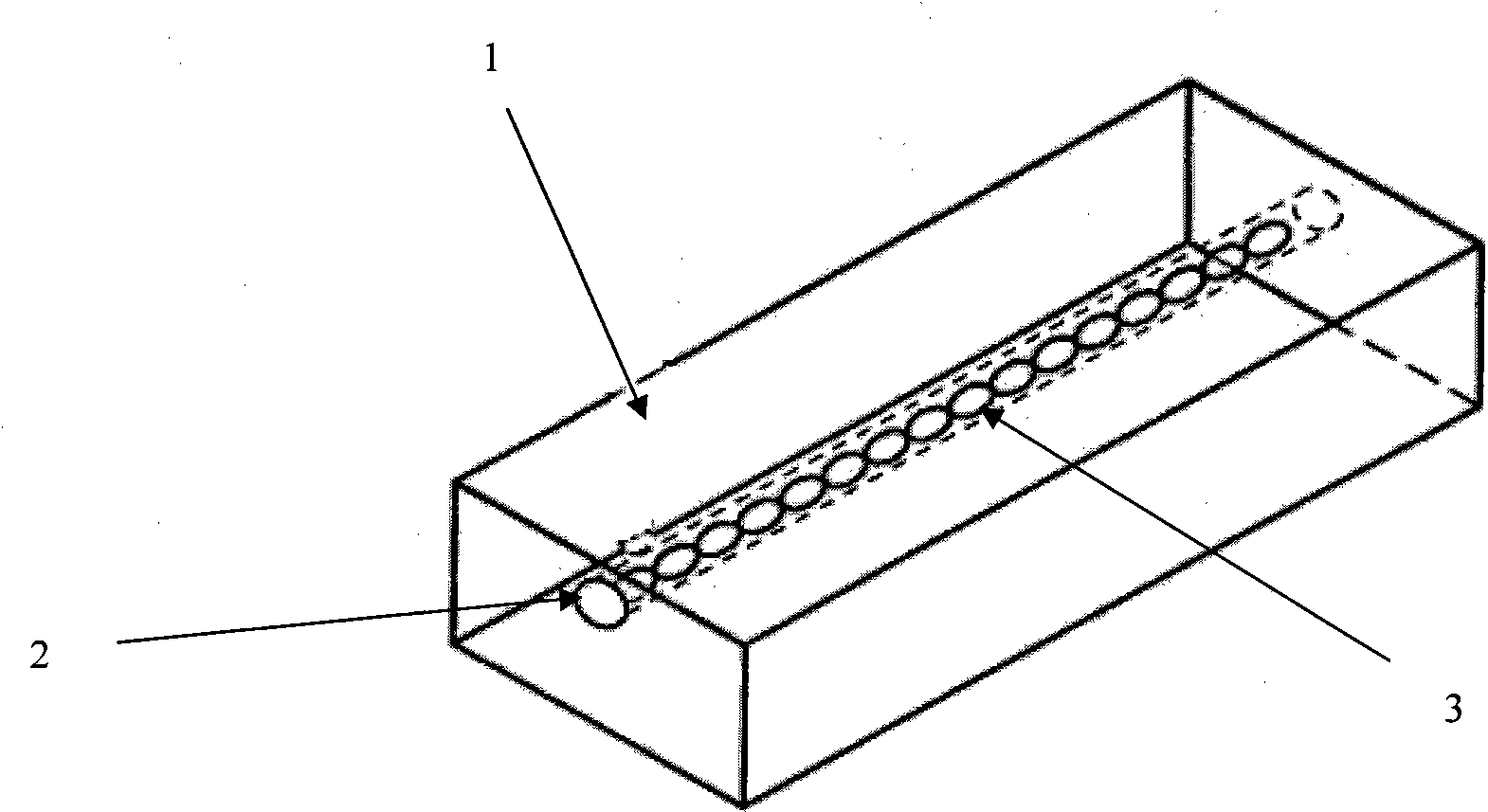
[0097] When the optical waveguide substrate 1 with the waveguide grating 3 becomes a packaged sensor 8 and is manufactured, one end is connected to an ordinary optical fiber 7 or a high-temperature-resistant optical fiber, and the other end is not connected to the optical fiber. After packaging, it is made A sensor can place a high-temperature-resistant optical waveguide device with a grating, such as a sapphire optical waveguide device with a grating, at a high temperature point as a high-temperature induction device. The temperature at a certain distance from the high-temperature area is lower, and it can An ordinary optical fiber 7 is used to transmit optical signals, and if it is in a high temperature area, a sapphire optical fiber can be used to transmit optical signals. An optical waveguide device with a grating, that is, a packaged sensor 8, is connected to a fiber coupler 9 through an optical fiber 7, and the other two ports of the fiber coupler 9 are respectively conne...

Embodiment 2

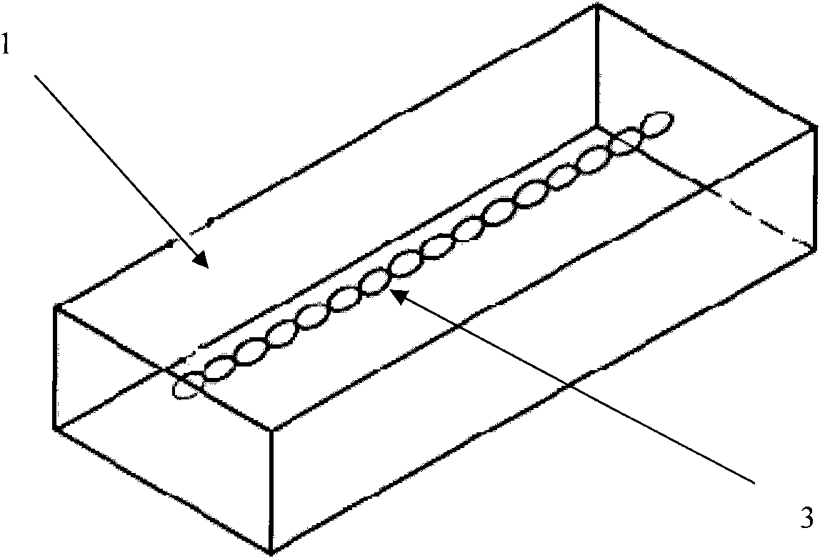
[0099] If both ends of the optical waveguide device with a grating are coupled to the optical fiber, the optical signal enters from one optical fiber and exits from the other optical fiber. This is the temperature of the optical waveguide device with a grating using a transmission method. As for the sensor device, the optical fiber can be an ordinary optical fiber, which is used in a low temperature area, or a sapphire optical fiber, which is used in a high temperature area.

Embodiment 3

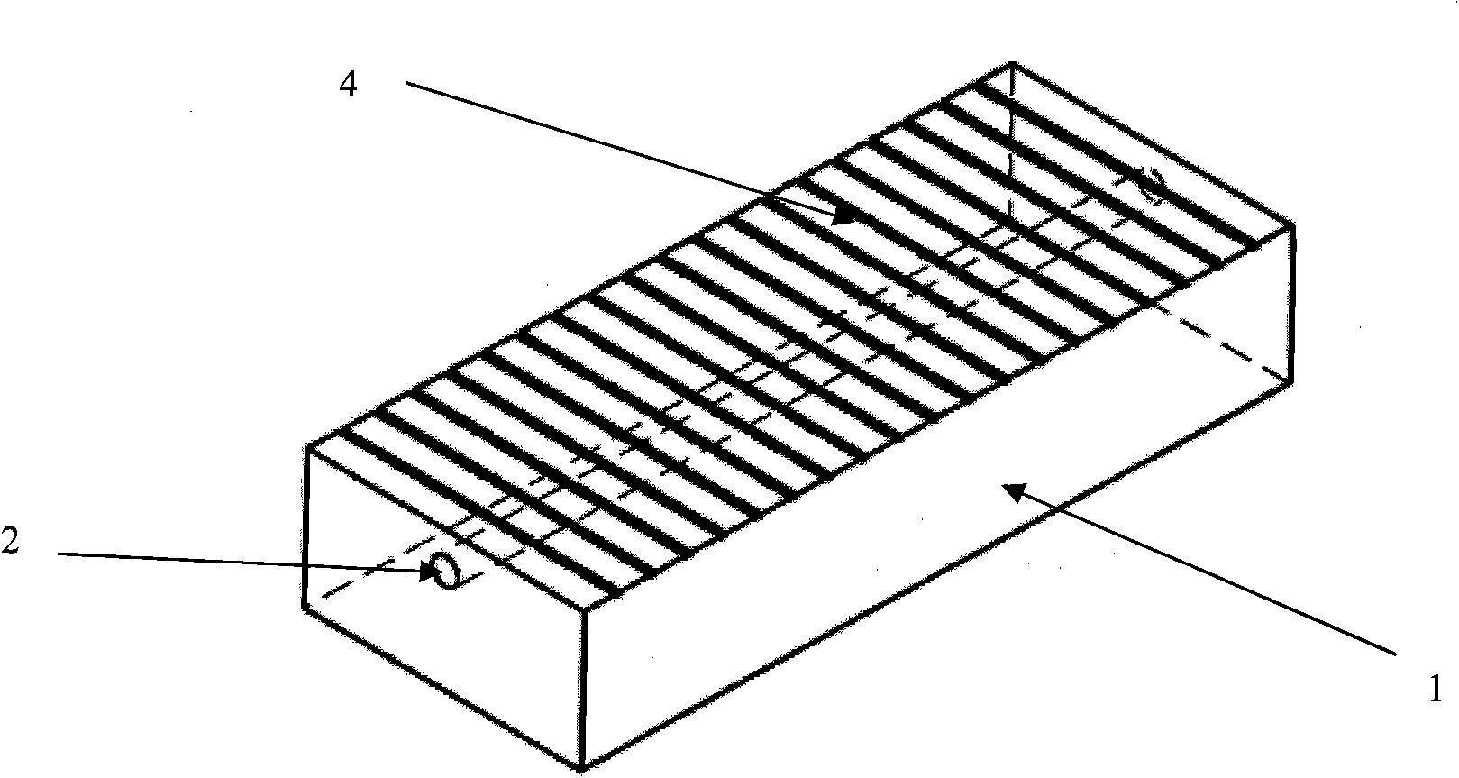
[0101] Write gratings at different positions of an optical waveguide device with a linear waveguide structure, and the grating period at each position is different, forming a distributed optical fiber sensor system that can measure temperature or other physical quantities at different positions.


PUM


Abstract

The invention discloses an optical waveguide sensor and preparation methods thereof. The optical waveguide sensor comprises a structure as follows: an optical waveguide substrate medium consists of heat resisting optical materials and is provided with linear optical waveguides, and in which an optical grating structure is arranged in the linear optical waveguides. The invention further discloses many preparation methods of the structure. Another waveguide sensor comprises a structure as follows: the optical waveguide substrate medium consists of heat resisting optical materials and is provided with linear optical waveguides, and an optical grating structure is further arranged on the surface of the optical waveguide substrate. The invention further discloses many preparation methods of the structure. Because the optical waveguide apparatus has a simple module structure or a structure with few modules, the optical grating on the optical waveguide channel only has a harmonic module or few modules. When the environment temperature is changed, the refractive index of the optical waveguide material and the period of the optical waveguide grating can be changed, therefore, the change of temperature can be measured by measuring the change of wavelength of harmonic wave of the optical grating in the optical waveguide channel on the optical waveguide substrate. Due to the adoption of the laser technology and microelectronic production process, a plurality of optical waveguide grating sensing apparatuses can be further produced on a same substrate with low production cost and high efficiency.

Description

technical field [0001] The invention belongs to the technical field of optical fiber sensing, and more specifically relates to an optical waveguide sensor and a manufacturing method thereof. Background technique [0002] Fiber Bragg grating is a good sensor for measuring physical quantities such as temperature and stress. When physical quantities such as temperature and stress change, the response of the grating in the optical fiber to the optical frequency also changes. By measuring the response change of the optical frequency of the fiber grating, the change of physical quantities such as temperature and stress can be measured. Fiber grating sensors have good characteristics, such as distributed, high sensitivity, anti-electromagnetic interference, and can work in harsh environments. [0003] The conventional fiber grating production method is to use ultraviolet light, two beams of light to interfere, or one beam of light to pass through a phase mask to generate two beams...

Claims


Application Information

Patent Timeline
IPC IPC(8): G01D5/26G02B6/34G01K11/32G01K11/3206
Inventor 龙品
Owner 无锡光芯科技有限公司
Why Eureka
Try Eureka