Semiconductor device structure and forming method thereof

A device structure and semiconductor technology, applied in the fields of semiconductor devices, semiconductor/solid-state device manufacturing, electrical components, etc., can solve problems such as difficulty, insignificant improvement in speed, and difficulty in realization, and achieve the effect of improving speed

Active Publication Date: 2010-09-15
TSINGHUA UNIV
View PDF4 Cites 55 Cited by
  • Summary
  • Abstract
  • Description
  • Claims
  • Application Information

AI Technical Summary

Problems solved by technology

[0002] At present, with the continuous shrinking of the feature size of the field effect transistor, its working speed is getting faster and faster, but the current feature size is close to the limit, so it will become more and more difficult to increase the speed by continuing to shrink the feature size. difficult and unattainable
Therefore, it is necessary to increase the speed of the device by other means, such as introducing stress to the channel material to achieve the purpose of increasing the mobility of carriers, but at present, this method does not significantly increase the speed and needs further improvement

Method used


Image

  • Semiconductor device structure and forming method thereof
  • Semiconductor device structure and forming method thereof
  • Semiconductor device structure and forming method thereof

Examples


Embodiment 1

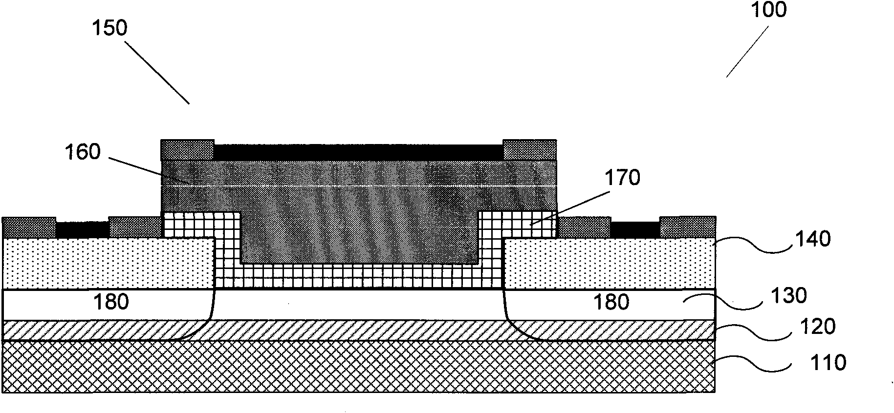
[0022] Such as figure 1 Shown is a structural diagram of a semiconductor device according to Embodiment 1 of the present invention. The semiconductor device structure 100 includes an insulating or semi-insulating substrate layer 110, an insulating substrate such as SiO 2 , silicon nitride, etc., and the semi-insulating substrate may include SiC or GaAs with a wide band gap. A silicon carbide layer (Silicon carbide layer) 120 formed on the insulating or semi-insulating substrate layer 110, and a carbon-based material layer 130 formed on the silicon-carbon layer 120, in one embodiment of the present invention, the carbon-based material Layer 130 may include a single layer or multiple layers of graphene. The semiconductor device structure 100 also includes a gate stack 150 formed on the carbon-based material layer 130, a source electrode and a drain electrode 180 formed in the carbon-based material layer 130, and a gate stack formed on the source electrode and the drain electro...

Embodiment 2

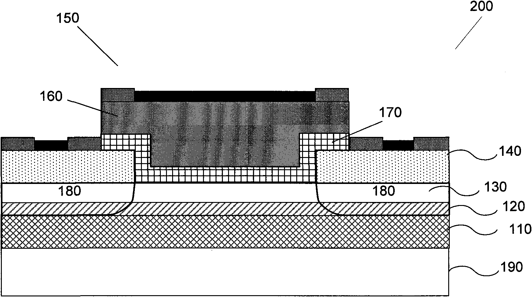
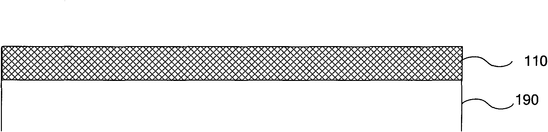
[0025] The present invention can also be formed on Si substrates, such as figure 2 Shown is a structural diagram of a semiconductor device according to Embodiment 2 of the present invention. This structure is similar to that of the first embodiment, except that the semiconductor device 200 further includes a Si substrate 190 in this embodiment. In one embodiment of the present invention, the Si substrate 190 may be an N-type Si substrate. It should be noted that, in this embodiment, the insulating substrate or semi-insulating substrate layer 110 of Embodiment 1 may not be required, for example, a silicon carbon layer may be directly grown on the Si substrate 190, and the silicon carbon layer A part of Si is fused with metal Ni to form the carbon-based material layer 130 and the metal silicide layer 140 , and the other part serves as the insulating or semi-insulating substrate layer 110 .

[0026] In order to more clearly understand the above-mentioned semiconductor structur...

Embodiment 3

[0037] Such as Figure 10 Shown is a structural diagram of a semiconductor device according to Embodiment 3 of the present invention. The semiconductor device structure 300 includes a substrate 310, a gate stack 320 formed on the substrate 310, one or more layers of sidewalls 360 formed on both sides of the gate stack 320, a source and a gate formed in the substrate 310. The drain 330 , and the silicon carbon layer 340 and the carbon-based material layer 350 formed under the gate stack 320 and in the substrate 310 . Wherein, the carbon-based material layer 350 is formed by annealing the silicon carbon layer and the metal layer, part of the Si in the silicon carbon layer fuses with the metal to form a metal silicide, and the remaining silicon carbon layer is the silicon carbon layer 340 . In one embodiment of the present invention, the metal layer may include, but not limited to, Ni, Al, Ti, Mo, W, Co, Pt, Pd, Ta or combinations thereof. In another embodiment of the present i...


PUM

PropertyMeasurementUnit
thicknessaaaaaaaaaa
thicknessaaaaaaaaaa
carrier mobilityaaaaaaaaaa

Abstract

The invention provides a semiconductor device structure and a forming method thereof. The semiconductor device structure comprises a substrate layer, a silicon carbon layer, a carbon base material layer, a gate stacker, a source, a drain and a metal silicide layer, wherein the silicon carbon layer is formed on the substrate layer; the carbon base material layer is formed on the silicon carbon layer; the gate stacker is formed on the carbon base material layer; the source and the drain are formed in the carbon base material layer; and the metal silicide layer is formed on the source and the drain. In the invention, the carbon base material layer, such as graphene, is used as a channel layer, and therefore, the speed of the device is greatly increased.

Description

technical field [0001] The invention relates to the technical field of semiconductor design and manufacture, in particular to a semiconductor device structure and a forming method thereof. Background technique [0002] At present, with the continuous shrinking of the feature size of the field effect transistor, its working speed is getting faster and faster, but the current feature size is close to the limit, so it will become more and more difficult to increase the speed by continuing to shrink the feature size. Difficult and unattainable. Therefore, it is necessary to increase the speed of the device through other methods, such as introducing stress to the channel material to increase the mobility of carriers, but the current method does not significantly improve the speed and needs further improvement. Contents of the invention [0003] The purpose of the present invention is to at least solve one of the above-mentioned technical defects, especially to propose a struct...

Claims


Application Information

Patent Timeline
Patent Type & Authority Applications(China)
IPC IPC(8): H01L29/78H01L29/12H01L21/336
Inventor 梁仁荣王敬许军
Owner TSINGHUA UNIV
Why Eureka
Try Eureka