Preparation method of absorption layer of thin film solar cell

A technology of solar cells and thin film layers, applied in the field of solar cells, can solve the problems of high process temperature, high production cost, affecting production efficiency, etc., and achieve the effect of improving the average deposition rate and increasing the production capacity

Active Publication Date: 2010-09-15
BEIJING NAURA MICROELECTRONICS EQUIP CO LTD
View PDF0 Cites 14 Cited by
  • Summary
  • Abstract
  • Description
  • Claims
  • Application Information

AI Technical Summary

Problems solved by technology

However, there are still some problems in the amorphous silicon and microcrystalline silicon stacked thin film battery itself: first, the interface problem, due to the introduction of the microcrystalline silicon layer, the number of heterojunction interfaces in the absorber layer increases, such as p-type microcrystalline silicon layer and The interface of the intrinsic microcrystalline silicon layer (p-i interface), due to the structure and composition mismatch on the interface (lattice constant mismatch), will cause the increase of series resistance, the decrease of photocurrent density, and the decrease of fill factor, etc. The second is the problem of the material of the absorbing layer itself. Fig. 2 is a schematic diagram of the microstructure of the amorphous silicon layer and the microcrystalline silicon layer material. As shown in the figure, there are many dangling bonds ( As shown by the black dots in the figure), it is necessary to introduce hydrogen atoms to satu

Method used


Image

  • Preparation method of absorption layer of thin film solar cell
  • Preparation method of absorption layer of thin film solar cell
  • Preparation method of absorption layer of thin film solar cell

Examples


Embodiment 1

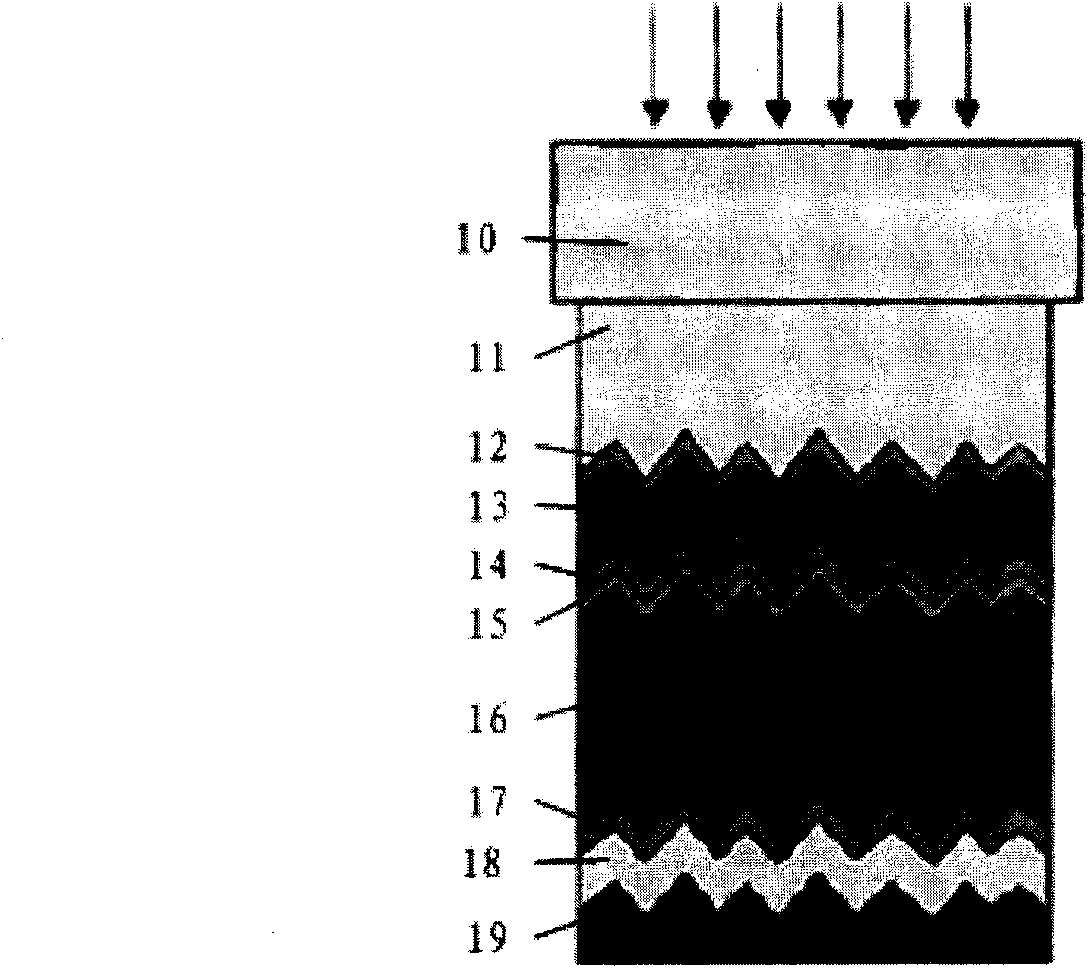
[0038] image 3 It is a flow chart of the preparation method of the absorbing layer of the thin film solar cell in this embodiment. Figure 4 to Figure 5 It is a schematic diagram of the preparation method of the absorbing layer of the thin-film solar cell in this embodiment.

[0039] Such as image 3 with Figure 4 As shown, step S1: providing a substrate 100 having a p-type silicon-based thin film layer 102 .

[0040] The substrate 100 can be a transparent conductive glass (ZnO-TCOGlass) with a ZnO texture film layer, and has an amorphous silicon (a-Si:H) absorption layer 101 on the substrate 100, and the amorphous silicon absorbs Layer 101 includes a p-i-n structure, that is, p-type amorphous silicon layer / intrinsic amorphous silicon layer / n-type amorphous silicon layer. The amorphous silicon absorption layer 101 is used in thin-film solar cells to absorb short-wave sunlight to generate photovoltaic effects. The amorphous silicon absorption layer 101 also has a p-type sil...

Embodiment 2

[0051] Image 6 It is a flow chart of the preparation method of the absorbing layer of the thin film solar cell in this embodiment.

[0052] Such as Image 6 As shown, step P1: providing a substrate with a p-type silicon-based thin film layer on the substrate;

[0053] Step P2: alternately performing hydrogenation treatment and depositing an intrinsic silicon-based thin film layer on the p-type silicon-based thin film layer. During this process, the deposition rate of the intrinsic silicon-based thin film layer gradually increases.

[0054] Specifically, the surface of the substrate with the p-type silicon-based thin film layer is hydrogenated for 3-30s, and then the intrinsic silicon-based thin film layer is deposited at the first deposition rate V1, and the deposition time is 10-100s , followed by hydrogenation treatment for 3-60s, and then depositing the intrinsic silicon-based thin film layer at the second deposition rate V2 for 10-100s, the second deposition rate being ...


PUM


Abstract

The invention provides a preparation method of an absorption layer of a thin film solar cell, comprising the following steps of: providing a substrate which is provided with a p-type silica-based thin film layer; and repeatedly and alternatively carrying out hydrogenation treatment on the p-type silica-based thin film layer and depositing an intrinsic silica-based thin film layer, wherein the hydrogenation treatment comprises hydrogen plasma treatment. In the preparation method, the hydrogenation treatment can enable dangling bonds in the p-type or intrinsic silica-based thin film layer to be saturated by hydrogen, which can effectively reduce the defect states at a p-i interface and inside the intrinsic silica-based thin film and ensures that the comprehensive performance of the absorption layer is optimized, thereby improving the cell property; secondly, the deposition rate of the intrinsic silica-based thin film layer gradually increases in the process of repeatedly and alternatively carrying out the hydrogenation treatment and depositing the intrinsic silica-based thin film layer, and the deposition rate of the intrinsic silica-based thin film layer in every deposition process is greater than the former deposition rate, therefore, the average deposition rate can be improved, and the manufacturing capacity of solar cells can be promoted.

Description

technical field [0001] The invention relates to the technical field of solar cells, in particular to a method for preparing an absorbing layer of a thin-film solar cell. Background technique [0002] At present, thin-film solar cells mainly include: amorphous silicon single-junction or double-junction thin-film batteries, amorphous silicon and microcrystalline silicon stacked thin-film batteries, and triple-junction silicon-based thin-film batteries. Material. Amorphous silicon thin-film batteries are relatively mature in industrialization and have low manufacturing costs, but there is a serious problem of efficiency attenuation; amorphous silicon and microcrystalline silicon stacked thin-film batteries have the characteristics of high efficiency and high stability, and have won a lot of attention in recent years. Rapid development. [0003] figure 1 It is a schematic diagram of an amorphous silicon and microcrystalline silicon stacked thin film battery, in which the stac...

Claims


Application Information

Patent Timeline
IPC IPC(8): H01L31/18H01L31/20
CPCY02P70/50
Inventor 徐亚伟
Owner BEIJING NAURA MICROELECTRONICS EQUIP CO LTD
Why Eureka
Try Eureka