Indium welded ball array preparing method based on electroplating technology

A solder ball array and electroplating technology, applied in circuits, electrical components, electrical solid devices, etc., can solve the problems of difficult process and little research, and achieve the effect of low cost and large scope of application

Inactive Publication Date: 2010-09-29
SHANGHAI INST OF MICROSYSTEM & INFORMATION TECH CHINESE ACAD OF SCI
View PDF3 Cites 11 Cited by
  • Summary
  • Abstract
  • Description
  • Claims
  • Application Information

AI Technical Summary

Problems solved by technology

However, this method is more difficult to process

Method used


Image

  • Indium welded ball array preparing method based on electroplating technology
  • Indium welded ball array preparing method based on electroplating technology
  • Indium welded ball array preparing method based on electroplating technology

Examples


Embodiment 1

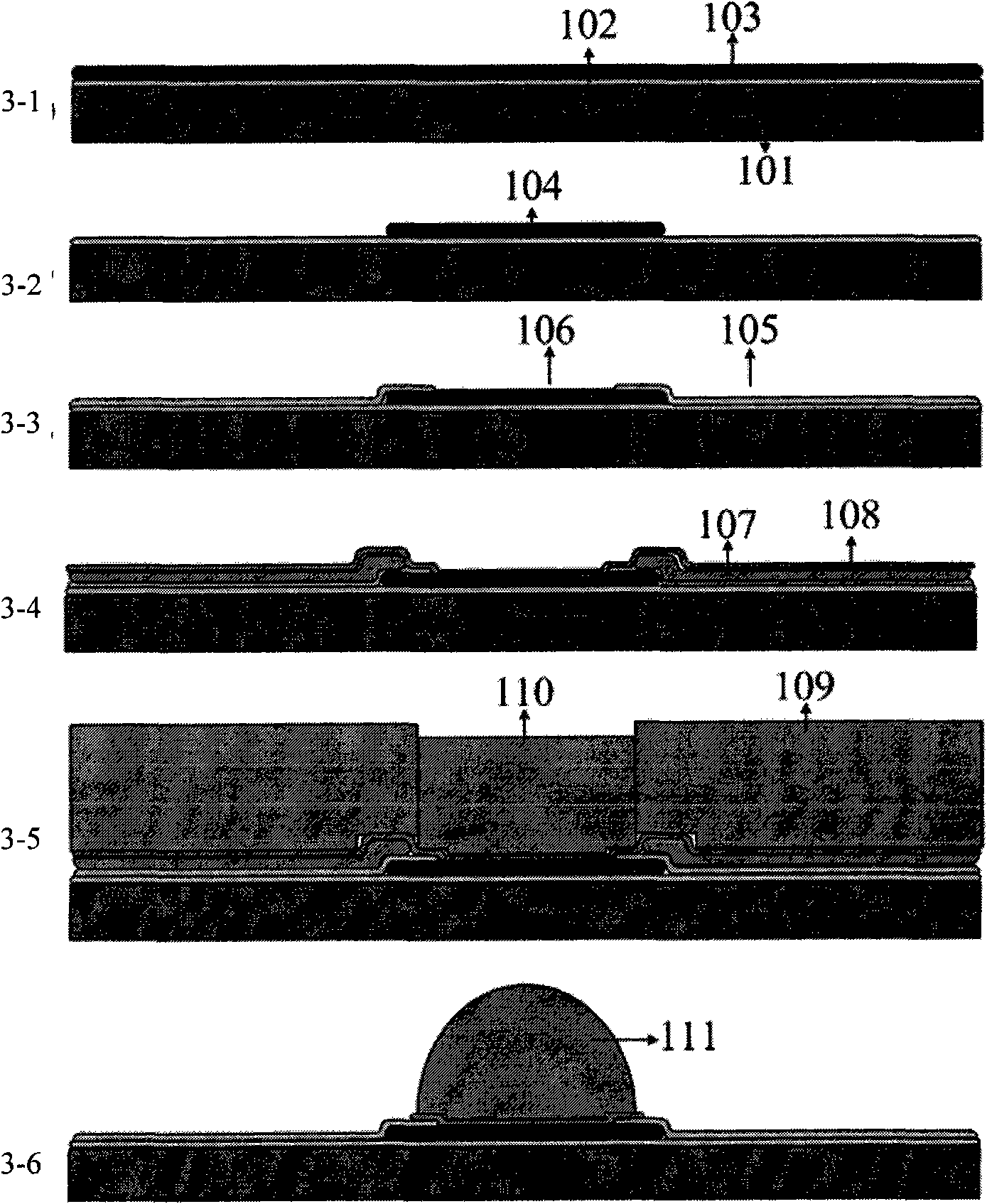
[0035] The concrete process step of embodiment 1 sees image 3 shown.

[0036] 1. With the silicon wafer 101 as the substrate, an oxide layer with a thickness of SiO 2 102 as an insulating layer, and then sputter a layer on it Thick Al layer 103; ( Figure 3-1 )

[0037] 2. Coating 1.7 μm of S1912 thin glue on the Al layer of the sputtering 103 and then photolithography, after the photolithography is completed, the pad 104 is etched out in the Al etching solution; ( Figure 3-2 )

[0038] 3. In order to protect the Al pad and prevent the indium solder ball from collapsing during reflow, it is necessary to use PECVD (ion-enhanced vapor deposition) to make a layer with a thickness of SiO 2 as the passivation layer 105. Then apply 1.7 μm S1912 thin glue again and photolithography, and then use RIE (reactive ion sputtering) to remove part of the SiO on the Al pad 104 2 To realize the passivation layer opening 106; ( Figure 3-3 )

[0039] 4. Apply S1912 thin glue agai...

Embodiment 2

[0043] The seed layer is Cr / Au or Ti / Ni / Au, and the rest are the same as in Example 1.


PUM

PropertyMeasurementUnit
Thicknessaaaaaaaaaa

Abstract

The invention relates to an indium welded ball array preparing method based on an electroplating technology, which is characterized in that primary thin photoresist lithography is carried out before a seed layer is manufactured, then the seed layer is manufactured, thick positive photoresist is coated at places where indium needs to be deposited to photoetch a mold and form a thin photoresist/seed layer/thick photoresist structure, an indium column with required height is deposited in the mold by an electroplating method, the seed layer is stripped by ultrasound, and finally indium salient point backflow is realized in an annealing furnace with a controllable temperature so as to obtain an indium welded ball array. The invention provides a novel seed layer removing technology by which high-quality indium welded balls with small distance, small size and large array are prepared successfully.

Description

technical field [0001] The invention relates to a method for preparing an array of indium solder balls, more specifically, to a method for preparing an array of indium solder balls based on an electroplating process. The indium solder ball array is mainly used for high-density interconnection between photoelectric devices, especially cooling focal plane devices, and silicon readout circuits, and belongs to the field of microelectronic packaging. Background technique [0002] In the process of fabricating cooled focal plane devices, a very critical technology is how to realize the interconnection between optoelectronic devices and silicon readout circuits. This kind of interconnection has the following two special requirements: (1) interconnection is realized at room temperature, and the device works at the ultra-low temperature of liquid nitrogen or liquid helium after interconnection; (2) high interconnection density: the higher the density, the final The imaging system im...

Claims


Application Information

Patent Timeline
IPC IPC(8): H01L21/60H01L31/18
CPCH01L24/11H01L2224/0361H01L2224/11H01L2224/1147H01L2224/11472
Inventor 黄秋平罗乐徐高卫袁媛
Owner SHANGHAI INST OF MICROSYSTEM & INFORMATION TECH CHINESE ACAD OF SCI
Why Eureka
Try Eureka