Method for making peripheral circuit device grid in flash memory

A peripheral circuit, flash memory technology, applied in circuits, electrical components, semiconductor devices, etc., can solve problems such as inability to obtain gates, failure of flash memory devices, and inability to pierce the polysilicon layer.

Inactive Publication Date: 2010-10-06
SEMICON MFG INT (SHANGHAI) CORP
View PDF1 Cites 16 Cited by
  • Summary
  • Abstract
  • Description
  • Claims
  • Application Information

AI Technical Summary

Problems solved by technology

[0016] As can be seen from the above description, due to the remaining second dielectric layer in the prior art, the polysilicon layer cannot be etched through during the process of etching the gate, so a complete gate can

Method used


Image

  • Method for making peripheral circuit device grid in flash memory
  • Method for making peripheral circuit device grid in flash memory
  • Method for making peripheral circuit device grid in flash memory

Examples


Embodiment Construction

[0032] The specific implementation of the method for fabricating gates of peripheral circuit devices in the flash memory provided by the present invention will be described in detail below with reference to the accompanying drawings.

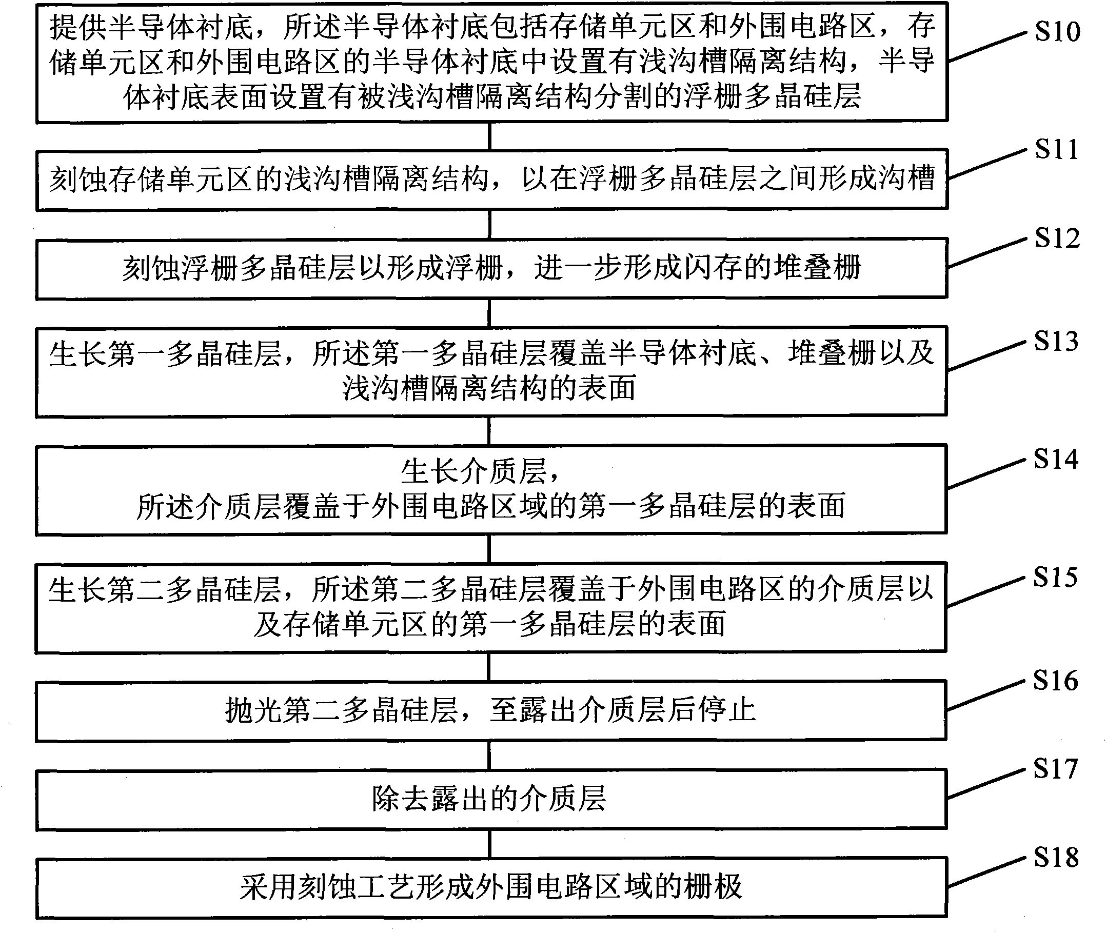
[0033] attached Figure 12 Shown is the flow chart of the implementation steps of this specific embodiment, including the following steps:

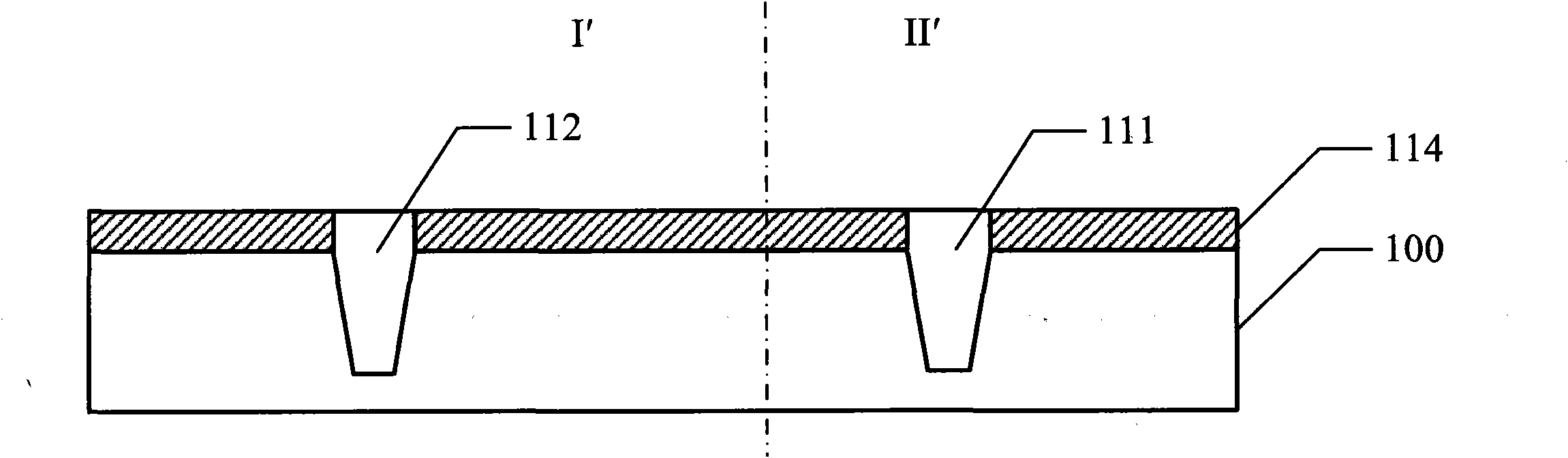
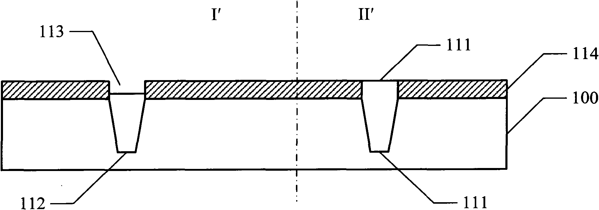
[0034]In step S20, a semiconductor substrate is provided, the semiconductor substrate includes a memory cell area and a peripheral circuit area, a shallow trench isolation structure is provided in the semiconductor substrate of the memory cell area and the peripheral circuit area, and shallow trench isolation structures are provided on the surface of the semiconductor substrate. The floating gate polysilicon layer separated by the trench isolation structure; step S21, etching the shallow trench isolation structure in the memory cell area to form a trench between the floating gate polysilicon layers, and sim...


PUM


Abstract

The invention provides a method for making a peripheral circuit device grid in a flash memory, comprising the following steps: providing a semi-conductor substrate, wherein the semi-conductor substrate comprises a storage unit area and a peripheral circuit area; etching a shallow trench isolation structure of the storage unit area; etching a floating-gate polysilicon layer to form a floating gate and further form a stack grid for the flash memory; growing a first polysilicon layer; growing a medium layer; growing a second polysilicon layer; polishing the second polysilicon layer; removing the exposed medium layer; forming the grid of the peripheral circuit area by an etching process; and etching the surface of the shallow trench isolation structure in the peripheral circuit area before growing the first polysilicon layer. The invention has the advantage that using an etching method reduces the height difference between the oxide surface of the shallow trench isolation structure and the silicon active area of an adjacent area within the range of over-corrosion depth of a polishing process, and ensures to obtain the complete grid in a subsequent process.

Description

【Technical field】 [0001] The invention relates to the field of integrated circuit manufacturing, in particular to a method for making gates of peripheral circuit devices in flash memory. 【Background technique】 [0002] Flash memory is a common integrated circuit storage device, which belongs to a non-volatile memory and is widely used in various occasions. The characteristic of non-volatile memory is that when the working voltage disappears, the memory can still save data for a long time without loss. [0003] Split-gate (Split-Gate) flash memory and stack-gate flash memory devices are two common flash memory devices. Compared with stacked gate flash memory devices, split gate flash memory has the advantages of small size and low power consumption. Regarding the manufacturing method of the split-gate flash memory, reference may be made to the content described in US Pat. No. 6,538,277. A typical flash memory chip includes memory cells and peripheral circuits. The devices...

Claims


Application Information

Patent Timeline
IPC IPC(8): H01L21/8247H01L21/28H01L21/311
Inventor 王友臻周儒领黄淇生詹奕鹏
Owner SEMICON MFG INT (SHANGHAI) CORP
Why Eureka
Try Eureka