Design method of two-dimensional photonic crystal waveguide coupler

A two-dimensional photonic crystal and design method technology, applied in the coupling of optical waveguides, instruments, optics, etc., can solve the problems of complex design structure, difficulty in adjusting the coupling distance, weak versatility, etc., to simplify the structure and improve the coupling distance Effect

Inactive Publication Date: 2010-10-13
NANJING UNIV OF SCI & TECH
View PDF2 Cites 14 Cited by
  • Summary
  • Abstract
  • Description
  • Claims
  • Application Information

AI Technical Summary

Problems solved by technology

In 2007, et al. first proposed to design a high-efficiency photonic crystal energy coupler by optimizing the structure of photonic crystals. However, due to the complexity of the design structure and the change of the structure of the original photonic crystal device, the method cannot achieve a general coupling design. And the coupling efficiency is only 87%
At present, there are still three main problems in the design of two-dimensional photonic crystal energy couplers at home and abroad: (1) the coupling cannot be realized without destroying the original structure; (2) the coupling distance is difficult to adjust; (3) the realization of The coupling structure is relatively limited and the versatility is weak; (4) the structure is complex; (5) the coupling efficiency is not high

Method used


Image

  • Design method of two-dimensional photonic crystal waveguide coupler
  • Design method of two-dimensional photonic crystal waveguide coupler
  • Design method of two-dimensional photonic crystal waveguide coupler

Examples


Embodiment 1

[0060] Embodiment 1: (Design of coupling between photonic crystal waveguides under the same lattice and the same unit cell)

[0061] (1) Determine the working wavelength λ=1550nm, select gallium arsenide as the dielectric column material, and air as the background dielectric material;

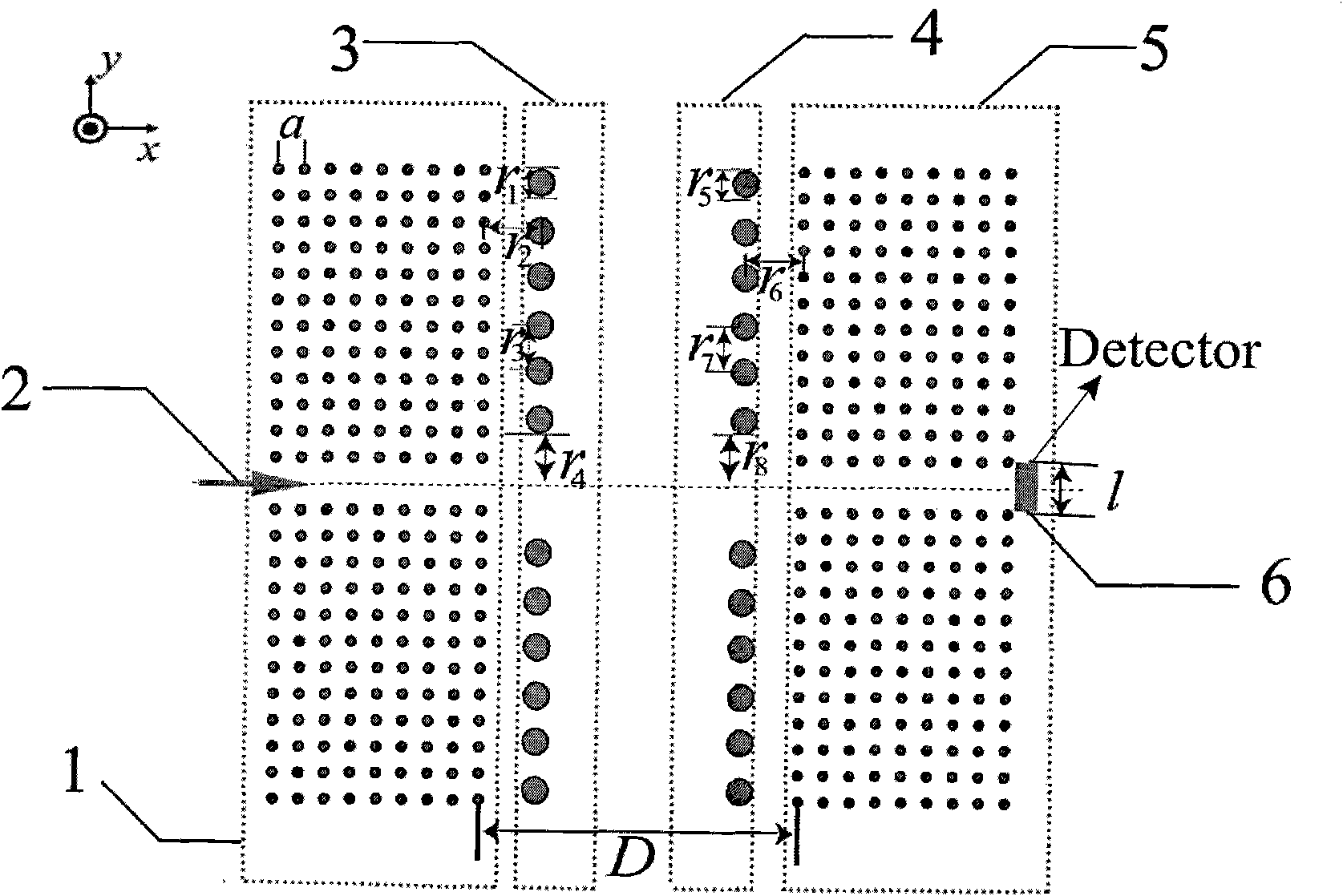
[0062] (2) Select the lattice constant a=0.35λ=542.5nm of the two-dimensional photonic crystal waveguide, and the distance D=12a between the exit surface of the outgoing waveguide and the entrance surface of the incident waveguide;

[0063] (3) Select the waveguide type as tetragonal lattice to realize waveguides between circular unit cells and circular unit cells, between square unit cells and square unit cells, and between hexagonal unit cells and hexagonal unit cells Coupling design, circular unit cell medium section diameter R=0.36a=195.2nm, square unit cell side length R=0.36a=195.2nm, hexagonal unit cell center symmetrical diagonal R=0.36a=195.2nm.

[0064] (4) A row of dielectric pillar...

Embodiment 2

[0072] Embodiment 2: (Design of different coupling distances of photonic crystal waveguide with tetragonal lattice cylindrical unit cell)

[0073] (1) Determine the working wavelength λ=1550nm, select gallium arsenide as the dielectric column material, and air as the background dielectric material;

[0074] (2) Choose both the outgoing waveguide and the incoming waveguide to be circular unit cells of tetragonal lattice. Its lattice constant a=0.35λ=542.5nm, the cross-section of the dielectric column is circular, and the cross-sectional dimension R=0.36a;

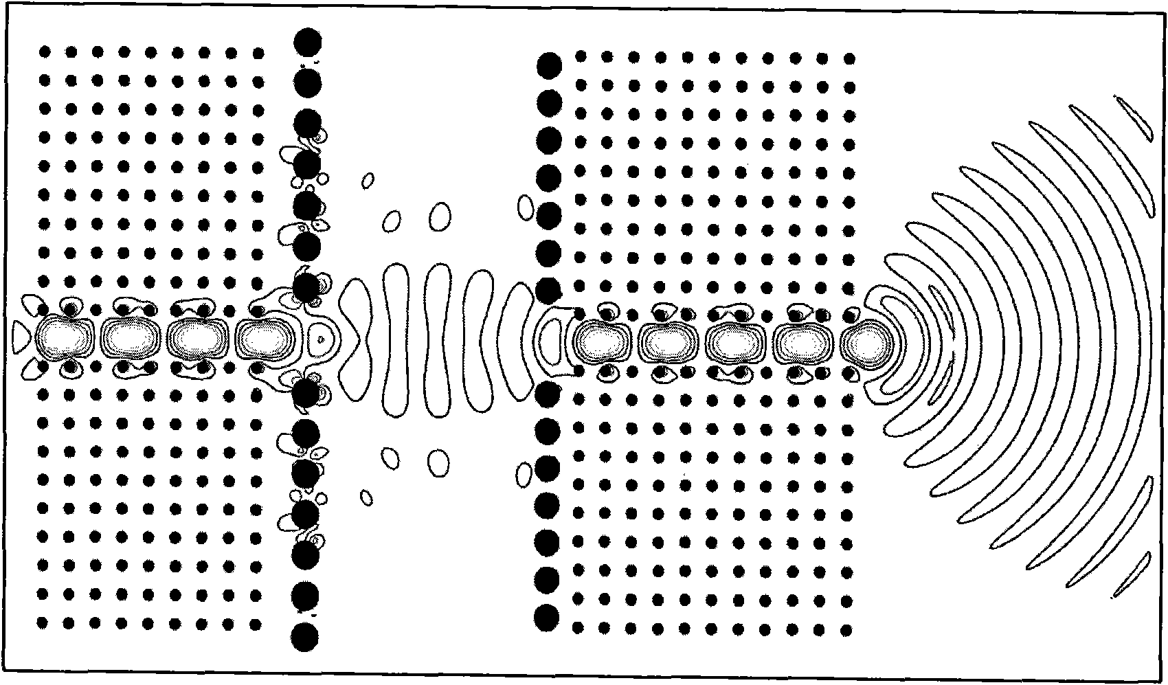
[0075] (3) The distance D between the exit surface of the outgoing waveguide and the entry surface of the incident waveguide is a variable, and we choose three coupling distances 12a, 14a, and 16a for design;

[0076] (4) repeat (4)~(8) step among the embodiment 1, obtain corresponding optimization parameter: as Figure 5 As shown, when the coupling distance is 12a, the waveguide modification surface parameters are: r1=0.5...

Embodiment 3

[0078] Embodiment 3: (Design of coupling between photonic crystal waveguides under different unit cells of the same lattice)

[0079] (1) Determine the working wavelength λ=1550nm, select gallium arsenide as the dielectric column material, and air as the background dielectric material;

[0080] (2) Choose both the outgoing waveguide and the incoming waveguide to be square lattices to realize waveguide energy coupling between circular unit cells and square unit cells, circular unit cells and hexagonal unit cells, and square unit cells and hexagonal unit cells . Its lattice constant is a=0.35λ=542.5nm, the diameter of the cross-section of the circular unit cell medium is R=0.36a, the side length of the square unit cell is R=0.36a, and the central symmetrical diagonal of the hexagonal unit cell is R=0.36a;

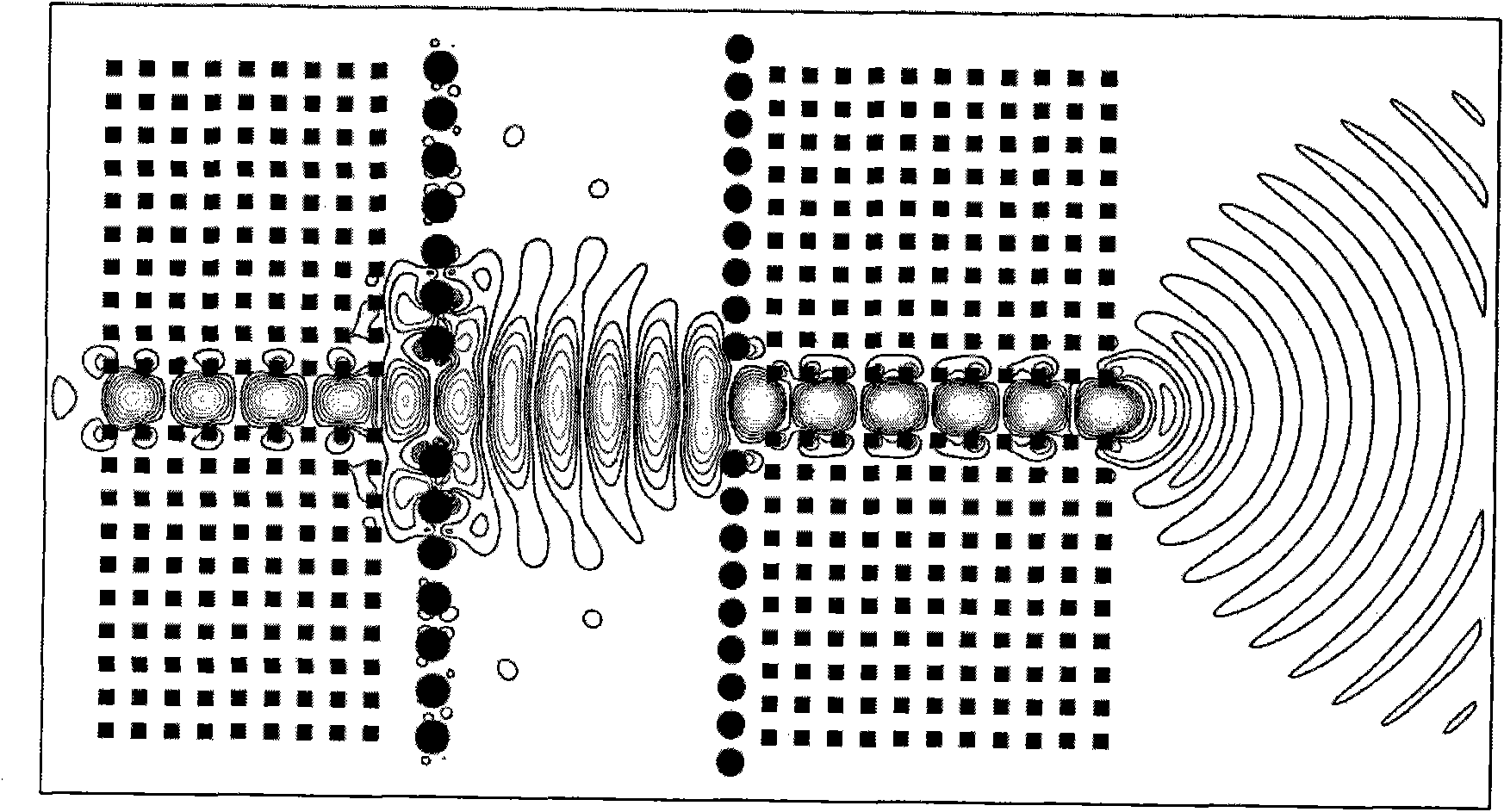
[0081] (3) The distance D between the exit surface of the outgoing waveguide and the entry surface of the incident waveguide is set to 12a;

[0082] (4) repeat (4)~(8) step...


PUM


Abstract

The invention relates to a design method of a two-dimensional photonic crystal waveguide coupler, which comprises the following steps: firstly selecting photonic crystal forbidden band waveguides with coincident waveguide mode frequencies, and enabling the waveguide passages of an emergent waveguide and an incident waveguide to be aligned on the same straight line; selecting an incident light frequency within the waveguide mode coincident frequency range of the two photonic crystal forbidden band waveguides; selecting the distance between the emergent waveguide and the incident waveguide according to the requirement of a photonic integrated device; respectively arranging a row of dielectric cylinders as a waveguide modifying surface in front of the emergent surface of the emergent waveguide and in front of the incident surface of the incident waveguide, and setting parameters to be optimized; arranging a detector at the guide opening of the incident waveguide, wherein the width of the detector is equal to the width of a PBG waveguide passage; and optimizing the parameters by utilizing a genetic algorithm to finish the design of the two-dimensional photonic crystal waveguide coupler. The method of the invention is simple and easy to operate, the coupling efficiency of the designed waveguide coupler is high, and the coupling distance can be adjusted within a certain range.

Description

technical field [0001] The invention relates to a photonic crystal waveguide and an integrated optical circuit device, in particular to a design method of a two-dimensional photonic crystal waveguide coupler. Background technique [0002] After the concept of photonic crystal was put forward, scholars launched a series of theoretical research on it. In 1990, He Qiming (Ho), Chen Ziting (Chan) and Soukoulis in the United States successfully predicted for the first time that there is a complete photon gap in a three-dimensional photonic crystal with a diamond structure, and the gap appears in the second and third Can take between. Then, in 1991, the research team led by Yablonovitch successfully produced the world's first artificial three-dimensional photonic crystal with a complete photonic band gap (band gap from 10 GHz to 13 GHz, located in the microwave field) by mechanical drilling method. Later known as "Yablonovitch" crystals. Since then, photonic crystals have becom...

Claims


Application Information

Patent Timeline
Patent Type & Authority Applications(China)
IPC IPC(8): G02B6/26G02B27/00
Inventor 贾巍蒋立勇李相银
Owner NANJING UNIV OF SCI & TECH
Why Eureka
Try Eureka