LED lead frame and electroplating method and electroplating equipment thereof

A lead frame, selective electroplating technology, applied in the direction of circuits, electrical components, semiconductor devices, etc., can solve the problems of affecting the quality of LED products, high production costs, low silver utilization, etc., to reduce the area of ​​electroplated silver layer and high production costs , The effect of reducing the cost of electroplating

Inactive Publication Date: 2010-10-20
XIAMEN YONGHONG TECH
View PDF5 Cites 29 Cited by
  • Summary
  • Abstract
  • Description
  • Claims
  • Application Information

AI Technical Summary

Problems solved by technology

[0015] Using the existing method of electroplating, the entire lead frame is electroplated with silver, and the non-functional area (frame) is also electroplated with silver. If there is no partial silver plating process in the functional area and only all electroplating is used, the thickness of the silver plating on the frame will be the same as that of the functional area. Thick, and, in order to ensure the silver plating thickness of the chip placement area, the silver plating thickness of the entire functional area is the same as that of the chip placement area, so that the utilization rate of silver is very low and the production cost is high
At the same time, the bonding force between the silver layer and the plastic is small, which may cause delamination between the silver layer and the plastic during customer packaging, affecting the quality of LED products

Method used


Image

  • LED lead frame and electroplating method and electroplating equipment thereof
  • LED lead frame and electroplating method and electroplating equipment thereof
  • LED lead frame and electroplating method and electroplating equipment thereof

Examples


Embodiment Construction

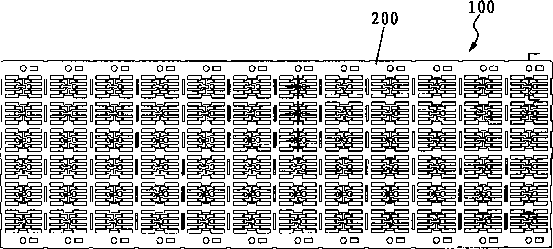
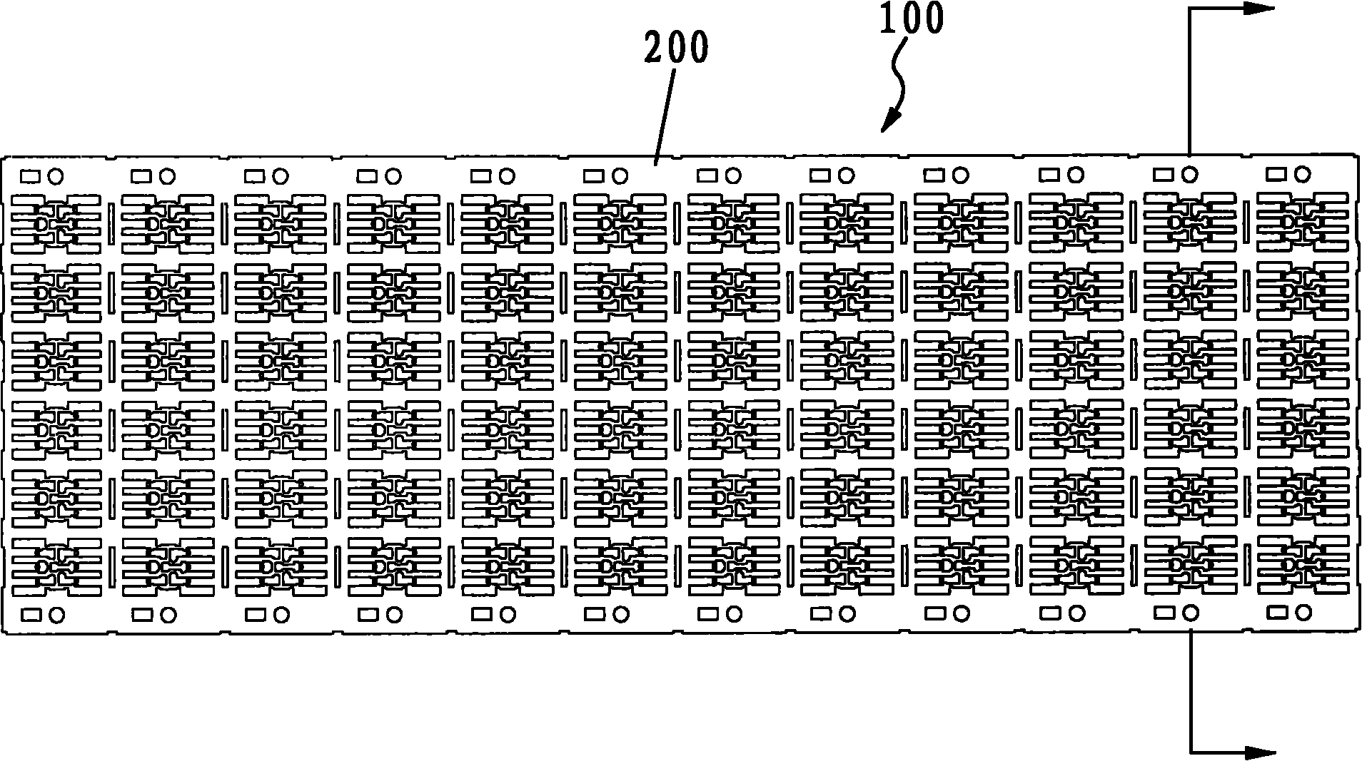
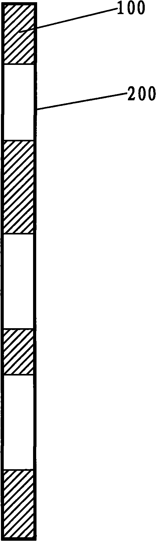
[0066] see Figure 5 to Figure 7 Shown is an LED lead frame 10 disclosed by the present invention, which is divided into three parts: a frame 11 , a functional area 12 and a chip placement area 13 . An anti-substitution protective film 14 is formed on the entire lead frame 10 . The primary silver plating layer 15 is formed on the entire functional area 12 through selective electroplating with silver. On the chip placement area 13, form secondary silver-plated layer 16 through partial electroplating silver again, make the silver-plated layer of chip placement area 13 (comprising silver-plated layer 15 and secondary silver-plated layer 16) than the silver-plated layer of surrounding functional area 12 layer (only one silver plating layer 15) is thick. An anti-copper oxidation organic protective film 17 is formed on the frame 11 .

[0067] Such as Figure 8 Shown, be the electroplating method of the LED lead frame that the present invention prompts, technological process is a...


PUM


Abstract

The invention discloses an LED lead frame which is divided into three parts, i.e. a side frame, a functional area and a chip placing area; an anti-replacement protective film is formed on the whole lead frame; a primary silver plated layer is formed on the whole functional area by selecting electroplating silver, and a secondary silver plated layer is formed on the chip placing area by local silver electroplating, so that the silver plated layer of the chip placing area is thicker than the silver plated layer of the functional area around; and an anti-copper oxidation organic protective film is formed on the side frame. The electroplating method comprises the following steps: chemical deoiling->electrolytic deoiling->water washing->acid washing->water washing->copper plating->water washing->anti-replacement treatment->water washing->electroplating silver selection for functional areas on the back side and on the front side->local silver electroplating of chip placing area->silver recovery->water washing->deplating->water washing->neutralization->water washing->anti-copper oxidization treatment->water washing->hot water washing->drying. The invention also discloses electroplating equipment. The invention can effectively use metal silver, reduces the cost, improves the bonding force between plastics and the lead frame, and achieves the purpose of anti-layering.

Description

technical field [0001] The invention relates to an LED lead frame, and relates to an electroplating method and equipment for the LED lead frame. Background technique [0002] In the prior art, the structure of the LED lead frame is as follows figure 1 , figure 2 with image 3 As shown, the entire lead frame 100 is entirely silver-plated 200 . [0003] Cooperate Figure 4 As shown, the electroplating process is as follows: chemical degreasing → electrolytic degreasing → water washing → pickling → water washing → copper plating → water washing → all electroplating silver (or all electroplating silver → partial electroplating silver in functional areas) → silver recovery → water washing →Deplating→Water washing→Neutralization→Water washing→Hot water washing→Drying, all of which are silver-plated for the entire lead frame. [0004] The role of each step in the process flow is as follows: [0005] Both chemical degreasing and electrolytic degreasing are used to remove grea...

Claims


Application Information

Patent Timeline
Patent Type & Authority Applications(China)
IPC IPC(8): H01L33/62C25D3/46C25D5/02C25D7/12
Inventor 林桂贤王锋涛龙海荣蔡智勇李志波
Owner XIAMEN YONGHONG TECH
Why Eureka
Try Eureka