Technique for manufacturing high-power light emitting diode (LED) lamp

An LED lamp and a manufacturing process technology, which are applied to parts of lighting devices, cooling/heating devices of lighting devices, optical elements for changing the spectral characteristics of emitted light, etc. Difficult to apply uniformly, difficult to control thickness, etc.

Inactive Publication Date: 2010-11-03
东莞市光宇新能源科技有限公司
View PDF1 Cites 30 Cited by
  • Summary
  • Abstract
  • Description
  • Claims
  • Application Information

AI Technical Summary

Problems solved by technology

At present, the commonly used coating method is: after the LED chip is soldered with wires, the phosphor is directly coated on the surface of the chip. In this way, the phosphor layer is difficult to coat evenly, and the thickness is difficult to control, resulting in low luminous efficiency of the LED lamp. The light color is not good; and the Chinese patent application No. 200710124607.0 discloses a phosphor coating process method for high-power LED chips. The powder glue is dotted on the surface of the LED chip, and the fluidity of the dam and the fluorescent powder glue is used to make it evenly coated. Although this method can solve the problem of uniform phosphor powder coating, it is very complicated to operate and has low efficiency. It is easy to damage its wires; in addition, the phosphor powder is directly in contact with the LED chip, which not only affects the heat dissipation and lighting brightness of the LED chip, but also the heat of the LED chip can easily accelerate the aging of the phosphor powder and reduce the effect of the phosphor powder, thereby making high-power Shortened lifespan of LED lamps

Method used


Image

  • Technique for manufacturing high-power light emitting diode (LED) lamp
  • Technique for manufacturing high-power light emitting diode (LED) lamp
  • Technique for manufacturing high-power light emitting diode (LED) lamp

Examples


Embodiment Construction

[0019] The present invention will be further described below in conjunction with specific embodiments and accompanying drawings.

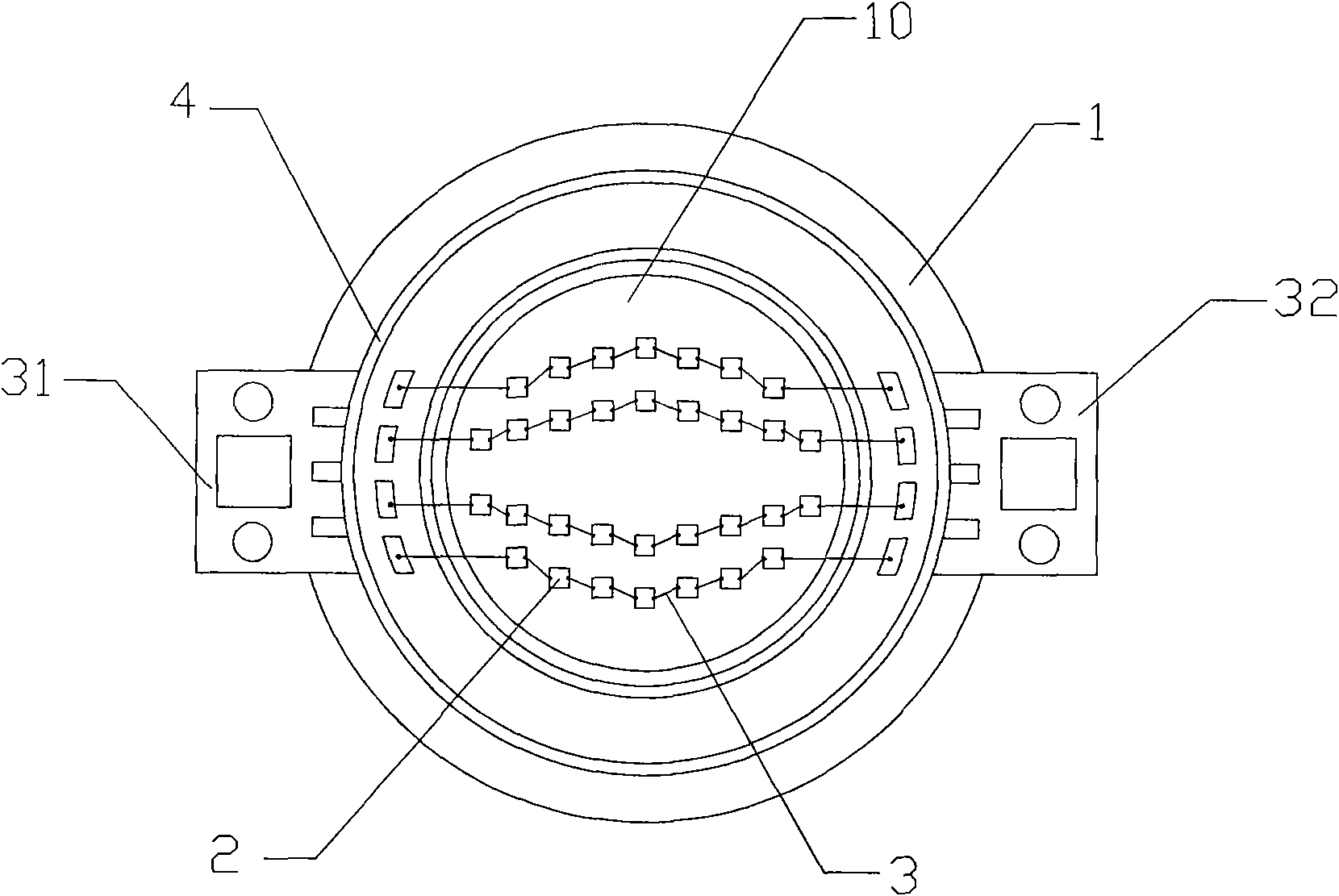
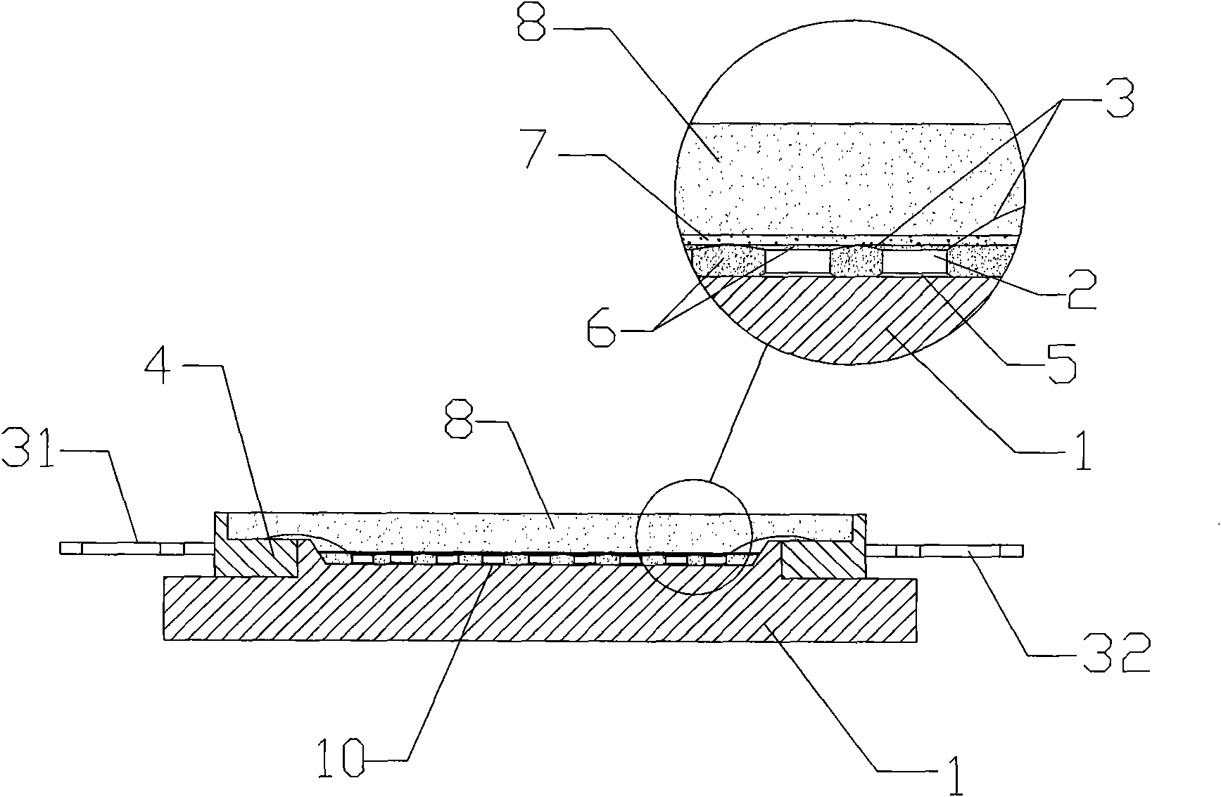
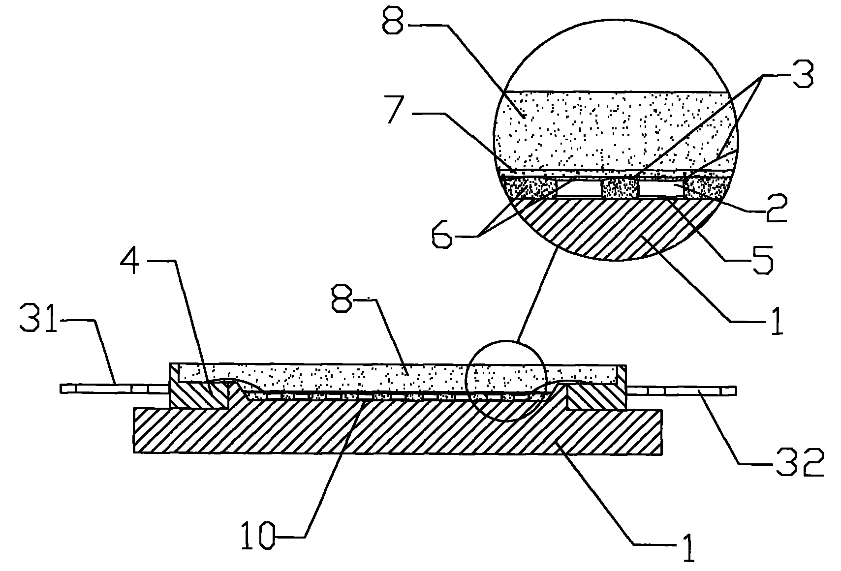
[0020] Such as figure 1 , 2 As shown, the high-power LED lamp of the present invention includes an LED bracket 1, the LED bracket 1 has a concave plane 10, the concave plane 10 is used to arrange a plurality of LED chips 2, the wires 3 between the LED chips 2, and the outermost wires 3 Connect the positive and negative pins 31 and 32 respectively; an insulating plastic frame 4 is provided around the concave plane 10 of the LED bracket 1, and the insulating plastic frame 4 is used to enclose the colloid during the packaging process to avoid spillage.

[0021] combine figure 2 As shown, the high-power LED lamp of the present invention is made through the following steps:

[0022] a. Point the silver glue 5 substrate on the surface of the LED bracket 1, place the LED chip 2 on the silver glue 5, and arrange the positive and negative poles of the L...


PUM


Abstract

The invention relates to the technical field of techniques for manufacturing light emitting diode (LED) lamps, in particular to a technique for manufacturing a high-power LED lamp. The technique comprises the following steps: die-bonding with fulmargin, welding the wires, sealing the primer, coating a fluorescent powder glue film, sealing finish, and the like, wherein the colloid in each step is dried in a sectional baking mode. After using the technical scheme, a LED chips is fixed with fulmargin, so that the LED chip can emit heat easily; before coating the fluorescent powder glue film, a layer of primer is sealed so as to tile and cover the fluorescent powder glue film on the LED chip, thereby avoiding the wires are damaged when the fluorescent powder is spotted, and isolating the fluorescent powder layer from the LED chip to avoid direct contact and be beneficial to deferring senility; and in addition, the primer, fluorescent powder glue film and finish are baked in a sectional mode, so that all the layers are uniform and can be well combined.

Description

Technical field: [0001] The invention relates to the technical field of manufacturing technology of LED lamps, in particular to a manufacturing technology of high-power LED lamps. Background technique: [0002] Due to its superior energy-saving properties, LED lamps are being used more and more widely. High-power LED lamps have a tendency to replace existing halogen street lamps as street lamps and other large-scale public lighting lamps. Generally speaking, large-scale public lighting requires the use of yellow light with good penetrability, while the existing yellow light LED lights mainly use blue LED chips and phosphors to excite yellow light, so the coating of phosphors It is one of the keys in the manufacturing process of high-power LED lamps. At present, the commonly used coating method is: after the LED chip is soldered with wires, the phosphor is directly coated on the surface of the chip. In this way, the phosphor layer is difficult to coat evenly, and the thickne...

Claims


Application Information

Patent Timeline
IPC IPC(8): F21S2/00F21V19/00F21V23/00F21V9/10H01L33/48H01L33/50H01L33/56H01L33/62F21Y101/02F21V9/40F21V29/10F21V29/503
CPCH01L2224/48137
Inventor 王骞
Owner 东莞市光宇新能源科技有限公司
Why Eureka
Try Eureka