
Epitaxy method for improving 4H-SiC basal plane dislocation conversion rate

A technology of basal plane dislocation and conversion rate, applied in the field of microelectronics, can solve the problems of reduced basal plane dislocation conversion rate, reduced device reliability, unclear growth mechanism, etc., to improve the conversion rate, simplify the process, and shorten the preparation. effect of cycles

Active Publication Date: 2011-09-21
陕西半导体先导技术中心有限公司
View PDF0 Cites 0 Cited by
  • Summary
  • Abstract
  • Description
  • Claims
  • Application Information

AI Technical Summary

Problems solved by technology

[0004] (1) Since there are two growth modes of lateral growth and step flow growth in the etching pit, when the lateral growth is dominant, the conversion rate of basal plane dislocations will increase, which will reduce the basal plane dislocation density, thereby improving the device performance. Reliability; when the step flow direction growth is dominant, the conversion rate of basal plane dislocations will be reduced, so that the basal plane dislocations generated in the substrate continue to extend into the epitaxial layer, reducing the reliability of the device;
[0005] (2) Since the microscopic growth mechanism is not yet clear, any growth mode in the etching pit is not easy to control in the process;
[0006] (3) Since polishing is required before secondary etching, more other defects will be introduced

Method used


Image

  • Epitaxy method for improving 4H-SiC basal plane dislocation conversion rate
  • Epitaxy method for improving 4H-SiC basal plane dislocation conversion rate
  • Epitaxy method for improving 4H-SiC basal plane dislocation conversion rate

Examples


Embodiment 1

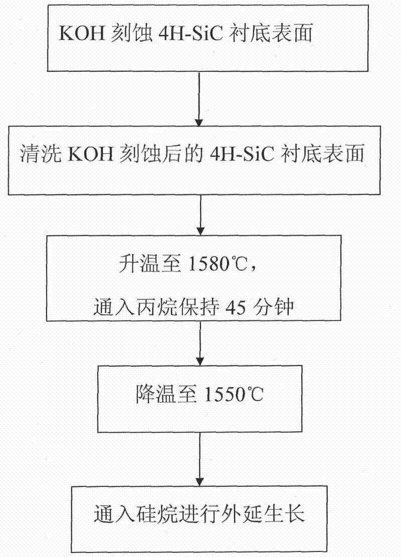
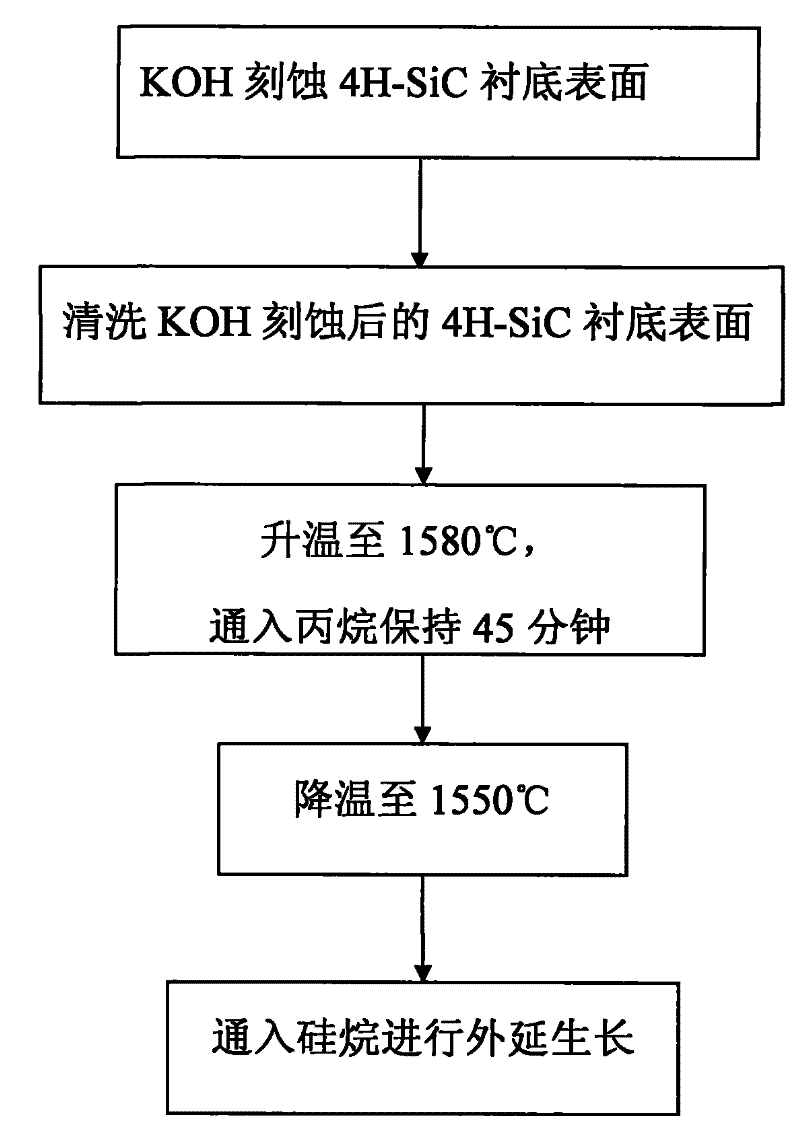
[0020] Embodiment 1, the implementation steps are as follows:

[0021] Step 1, the substrate is etched with KOH, the etching temperature is 480°C, and the etching time is 20min. The etched structure is as follows figure 2 shown.

[0022] Step 2: Clean the etched substrate surface with ethanol for the first cleaning to remove organic matter; use HF for the second cleaning of the etched substrate surface to remove ionic and atomic impurities; use high-purity water Carry out the third surface cleaning to ensure that the substrate surface is clean, and finally dry the surface moisture.

[0023] Step 3, place the cleaned 4H-SiC substrate in the CVD furnace cavity, and vacuumize the furnace so that the pressure in the furnace reaches 10 -7 Pa, raise the temperature in the furnace, and at the same time, feed hydrogen gas with a flow rate of 20l / min, raise the temperature to 1400°C, keep it for 5min, then feed it with a flow rate of 8ml / min propane, raise the temperature to 1580°C, ...

Embodiment 2

[0025] Embodiment 2, the implementation steps are as follows:

[0026] In step 1, the substrate is etched with KOH, the etching temperature is 520° C., and the etching time is 10 min.

[0027] Step 2: Clean the etched substrate surface with ethanol for the first cleaning to remove organic matter; use HF for the second cleaning of the etched substrate surface to remove ionic and atomic impurities; use high-purity water Carry out the third surface cleaning to ensure that the substrate surface is clean, and finally dry the surface moisture.

[0028] Step 3, place the cleaned 4H-SiC substrate in the CVD furnace cavity, and vacuumize the furnace so that the pressure in the furnace reaches 10 -7 Pa, raise the temperature in the furnace, and at the same time feed hydrogen with a flow rate of 50l / min, raise the temperature to 1500°C, keep it for 5min, then feed it with a flow rate of 15ml / min propane, raise the temperature to 1600°C, and keep it at a pressure of 100mbar for 30 minute...

Embodiment 3

[0030] Embodiment 3, the implementation steps are as follows:

[0031] In step 1, the substrate is etched with KOH, the etching temperature is 490° C., and the etching time is 15 minutes.

[0032] Step 2: Clean the etched substrate surface with ethanol for the first cleaning to remove organic matter; use HF to clean the etched substrate surface for the second time to remove ionic and atomic impurities; use high-purity water Carry out the third surface cleaning to ensure that the substrate surface is clean, and finally dry the surface moisture.

[0033] Step 3, place the cleaned 4H-SiC substrate in the CVD furnace cavity, and vacuumize the furnace so that the pressure in the furnace reaches 10 -7 Pa, raise the temperature in the furnace, and at the same time feed hydrogen with a flow rate of 30l / min, raise the temperature to 1450°C, keep it for 5min, then feed it with a flow rate of 10ml / min propane, raise the temperature to 1590°C, and keep it at a pressure of 90mbar for 45 m...


PUM


Abstract

The invention discuses an epitaxy method for improving 4H-SiC basal plane dislocation conversion rate, which mainly solves the problem that the conversion rate that basal plane dislocation is converted into edge forming dislocation is low by adopting an corrosion method; the method comprises the following steps: (1) etch a 4H-SiC substrate by KOH, the etching temperature is 480-520 DEG C, and theetching time is 10-20min; (2) surface cleaning processing is carried out to the etched 4H-SiC substrate; (3) a 4H-SiC sample which carries out surface cleaning processing is placed in a CVD furnace cavity, vacuumizing is carried out to lead the pressure intensity in the furnace to reach 10-7Pa, the temperature in the furnace is raised to 1400-1500 DEG C, and hydrogen with 20-50l / min flow rate flows in for 5min, and then 8-15ml / min of propane flows in, the temperature is raised to 1580-1600 DEG C for 30-50 minutes under 80-100mbar of pressure; (4) when the temperature is reduced to 1550 plus / minus 5 under the condition of unchanged pressure, and epitaxy growth is carried out by silane flowing-in. the method can be applied to manufacturing of 4H-SiC homoepitaxy material.

Description

technical field [0001] The invention belongs to the technical field of microelectronics and relates to the manufacture of semiconductor materials, in particular to an improved epitaxy method for minimizing defects in silicon carbide crystals, which can be used in the manufacture of semiconductor device materials. Background technique [0002] Silicon carbide (SiC) has great potential for making various high-frequency and high-power devices with high temperature resistance due to its characteristics such as large band gap, high breakdown electric field, good thermal stability, high electron mobility and high electron saturation drift velocity. Semiconductor materials for applications where silicon devices are incapable. With the development of SiC epitaxial growth technology, the micropipe defect of the wafer is reduced to 1 / cm 2 , which has become the biggest opportunity for the development of SiC high-frequency power devices. At present, the main problem of SiC epitaxial ...

Claims


Application Information

Patent Timeline
Patent Type & Authority Patents(China)
IPC IPC(8): H01L21/205H01L21/306H01L21/324
Inventor 苗瑞霞张玉明汤晓艳张义门
Owner 陕西半导体先导技术中心有限公司
Learn More