Surface plasma nanometer laser

A surface plasmon and laser technology, applied in phonon exciters, electrical components, circuits, etc., can solve the problems of difficult optical waveguide integration, complex processing and manufacturing processes, etc., and achieve the effect of low transmission loss

Inactive Publication Date: 2010-11-10
BEIHANG UNIV
View PDF6 Cites 28 Cited by
  • Summary
  • Abstract
  • Description
  • Claims
  • Application Information

AI Technical Summary

Problems solved by technology

[0008] The purpose of the present invention is to overcome the defects that the existing surface plasmon nanolaser based on the multilayer waveguide structure is relatively complex and difficult to realize the integration with the planar optical waveguide, and propose an edge-coupled surface plasmon nanolaser

Method used


Image

  • Surface plasma nanometer laser
  • Surface plasma nanometer laser
  • Surface plasma nanometer laser

Examples


example

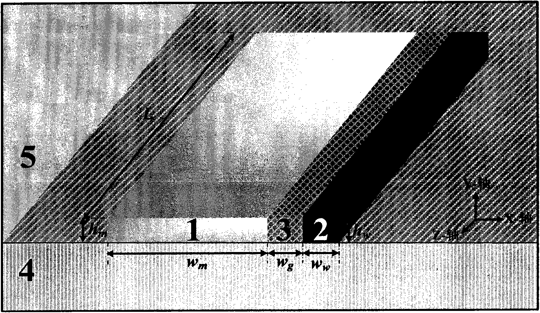
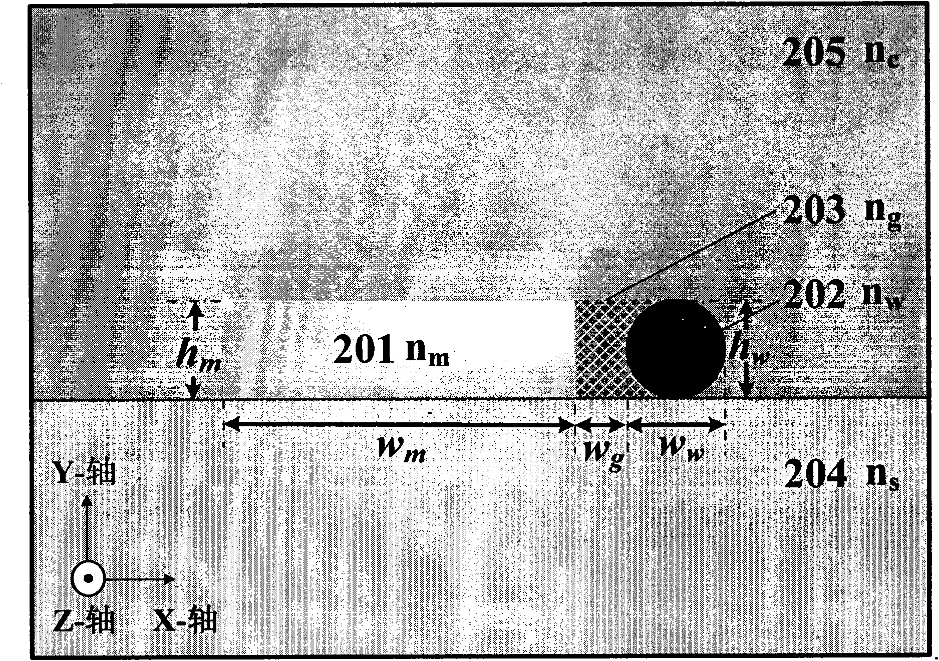
[0037] figure 2 is the cross-sectional structure diagram of the surface plasmon laser described in the example. 201 is a metal film layer, n m is its refractive index, w m its width, h m Its height; 202 is a cylindrical nanowire (end face is circular), located on the side of the edge on the right side of 201 (that is, along the positive direction of the X axis) and parallel to the edge on the right side of 201, n w is its refractive index, w w its width, h w Its height; 203 is the gap area between 201 and 202, n g is its refractive index; w g is the minimum distance from the left edge of 202 to the right edge of 201; 204 is the base layer, n s is its refractive index; 205 is the cladding, n c for its refractive index.

[0038] In this example, the wavelength of the laser output light is 490nm, the material of 201 is gold, the real part of the refractive index at the wavelength of 490nm is -9.2, and the imaginary part is 0.3; the material of 202 is cadmium sulfide, an...


PUM


Abstract

The invention discloses an edge-coupled surface plasma nanometer laser, which comprises a basal lamina (4), a metal film layer (1) which is arranged above the basal lamina, a gain medium nano-wire (2) which is arranged at one side on the lateral edge of the metal film layer and is parallel thereto, a gap area (3) which is arranged between the lateral edge of the metal film layer and the gain medium nano-wire and a cladding (5). The coupling between the gain medium nano-wire (2) and the lateral edge of the metal film layer (1) can remarkably limit the distribution of an optical field so as to realize the restriction of two-dimensional sub-wavelength of the optical field outputted by the laser and also to maintain the lower transmission loss. The surface plasma nanometer laser overcomes the defects of the surface plasma nanometer laser based on the multi-layer structure that the processing production technology is relatively complicated and the integration between the laser and the planar optical waveguide is difficult to realize, so the planar integration of nanometer active device can be realized.

Description

technical field [0001] The invention relates to the field of micro-nano photonic devices / lasers, in particular to a surface plasmon nano-laser. Background technique [0002] As one of the three great inventions of the 20th century, laser has developed rapidly in recent decades. With the rise of nanotechnology, the study of nanolasers has become a new and important topic. Nanolasers have strong application value in many fields, including electronic communication, information storage, biochemical sensors, and nanolithography. [0003] In recent years, lasers based on semiconductor nanowires such as zinc oxide, cadmium sulfide, and gallium nitride have attracted extensive attention from researchers. By introducing semiconductor nanowires and nanoarrays, current microlasers have reached the diffraction-limited level. In these lasers, semiconductor nanowires not only serve as the gain medium but also host the laser resonator. The earliest nanolaser was manufactured by the Uni...

Claims


Application Information

Patent Timeline
Patent Type & Authority Applications(China)
IPC IPC(8): H01S4/00
Inventor 郑铮卞宇生刘娅
Owner BEIHANG UNIV
Why Eureka
Try Eureka