

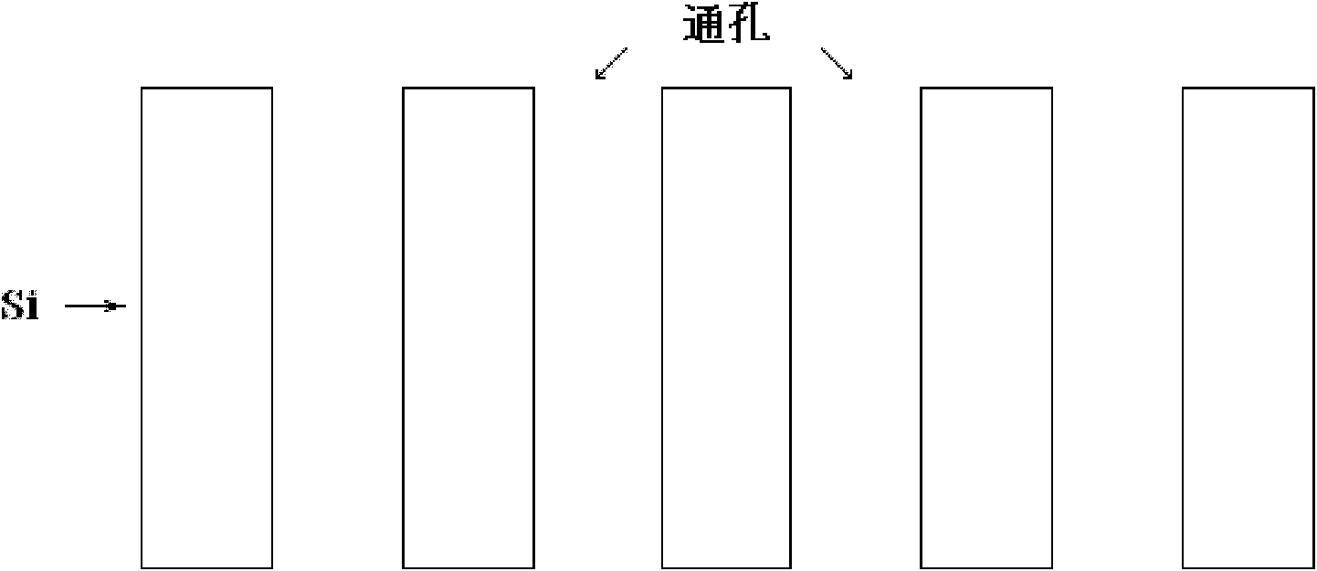
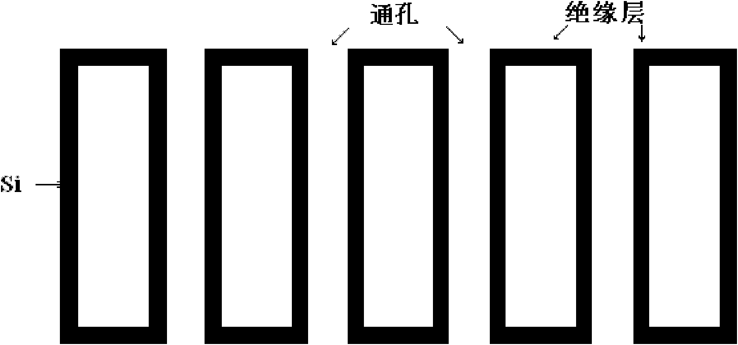
Ultrathin film wet preparation method for TSV insulating layer
An ultra-thin film and insulating layer technology, applied in the field of microelectronic materials, can solve the problems of complex process, poor step coverage, high cost of insulating layer, and achieve the effect of simple process flow, low cost and good combination.
- Summary
- Abstract
- Description
- Claims
- Application Information
AI Technical Summary
Problems solved by technology
Method used
Image


Examples
Embodiment 1
[0031] Preparation of Ultrathin Insulating Film of Polyurethane Modified Epoxy Resin
[0032] This embodiment adopts cathodic electrophoretic coating process, and uses polyurethane modified epoxy resin electrophoretic coating, which specifically includes the following steps:
[0033] (1) Connect the silicon wafer to be processed to the conductive device, the conductive device is connected to the negative pole of the power supply, and the anode of the electrophoresis device is connected to the positive pole of the power supply as an anode system.
[0034] (2) Put the silicon wafer into the electrophoretic coating solution containing 10% polyurethane modified epoxy resin, under the condition of 25°C, apply ultrasonic oscillation with a frequency of 25KHZ, the rotational speed of the rotating electrode is 50rmp, and the electrophoretic voltage is set to 30V , cathodic electrophoresis 10S.
[0035] (3) After the electrophoretic coating is completed according to the required time,...
Embodiment 2
[0039] Preparation of Ultrathin Insulating Film of Modified Acrylic Polyurethane Resin
[0040] This embodiment adopts cathodic electrophoretic coating process, uses modified acrylic polyurethane resin coating, specifically comprises the following steps:
[0041] (1) Connect the silicon wafer to be processed to the conductive device, the conductive device is connected to the negative pole of the power supply, and the anode of the electrophoresis device is connected to the positive pole of the power supply as an anode system.
[0042] (2) Put the silicon wafer into the electrophoretic coating solution containing 20% modified acrylic polyurethane resin, and under the condition of 25°C, apply ultrasonic oscillation with a frequency of 50KHZ, the rotational speed of the rotating electrode is 200rmp, and the electrophoretic voltage is set to 45V. Cathodic electrophoresis 30S.
[0043] (3) After the electrophoretic coating is completed according to the required time, the silicon ...
Embodiment 3
[0047] Preparation of Ultrathin Insulating Film of Acrylic Modified Epoxy Resin
[0048] This embodiment adopts the anodic electrophoretic coating process, and uses acrylic modified epoxy resin electrophoretic coating, which specifically includes the following steps:
[0049] (1) Connect the silicon wafer to be processed to the conductive device, the conductive device is connected to the positive pole of the power supply, and the cathode of the electrophoresis device is connected to the negative pole of the power supply as the cathode system.
[0050](2) Put the silicon wafer into the electrophoretic coating solution containing 30% acrylic modified epoxy resin, under the condition of 30°C, apply ultrasonic oscillation with a frequency of 68KHZ, the rotational speed of the rotating electrode is 300rmp, and the electrophoretic voltage is set to 60V , anodic electrophoresis 60S.
[0051] (3) After the electrophoretic coating is completed according to the required time, the silic...
PUM
| Property | Measurement | Unit |
|---|---|---|
| thickness | aaaaa | aaaaa |
| thickness | aaaaa | aaaaa |
| thickness | aaaaa | aaaaa |
Abstract
Description
Claims
Application Information