
Method for preparing silicon detector with high photoelectric response at room temperature

A photoelectric response and detector technology, applied in circuits, electrical components, semiconductor devices, etc., can solve problems such as difficulties and inability to detect photons, and achieve the effects of avoiding the formation of crystal cones, improving the scope of application, and improving sensitivity.

Inactive Publication Date: 2010-11-17
INST OF SEMICONDUCTORS - CHINESE ACAD OF SCI
View PDF0 Cites 9 Cited by
  • Summary
  • Abstract
  • Description
  • Claims
  • Application Information

AI Technical Summary

Problems solved by technology

Both types involve the Si forbidden band 1.12eV, and photons with energies below 1.12eV (wavelength greater than 1.1μm) cannot be detected
If you want to use Si to detect infrared light with an energy lower than 1.12eV, you must use the photoconductive properties of Si at low temperature, which brings great difficulties to practical use.

Method used


Image

  • Method for preparing silicon detector with high photoelectric response at room temperature
  • Method for preparing silicon detector with high photoelectric response at room temperature
  • Method for preparing silicon detector with high photoelectric response at room temperature

Examples


Embodiment

[0077] The ionized elements are separated by ion implantation equipment mass spectrometer, and then through vertical high-voltage acceleration and lateral bias scanning, the uniform distribution of single impurity elements in the horizontal direction of the Si surface and the non-equilibrium doping in the vertical direction are realized.

[0078] Or scan the Si surface in the impurity atmosphere by laser to realize the uniform distribution of a single impurity element in the lateral direction of the Si surface layer and the non-equilibrium doping in the vertical direction.

[0079] Or evenly heat the Si sheet in the furnace body at high temperature, and at the same time impurity atmosphere enters at a constant speed, so that impurity elements are doped into the surface layer of the Si sheet, and a single impurity element is uniformly distributed in the lateral direction of the Si surface layer and balanced in the vertical direction.

[0080] The above-mentioned doping impurity ...


PUM


Abstract

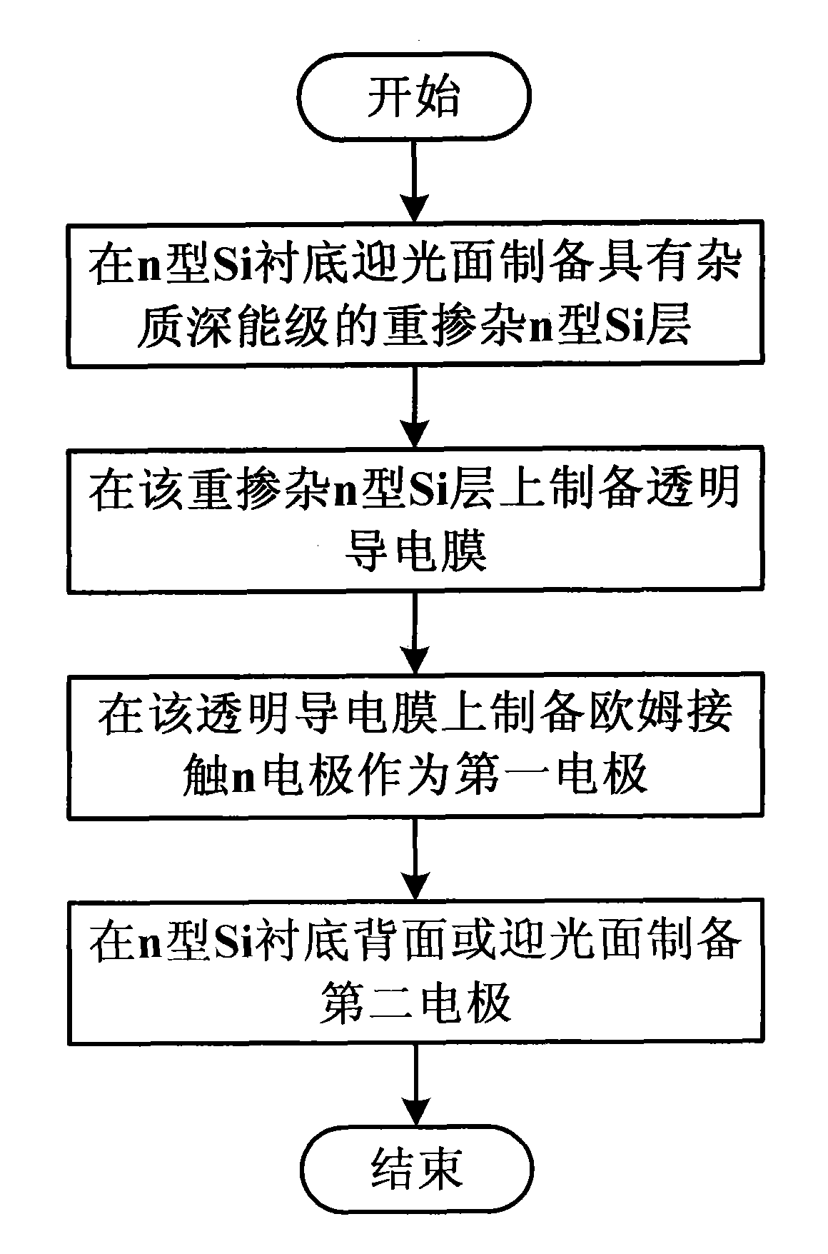
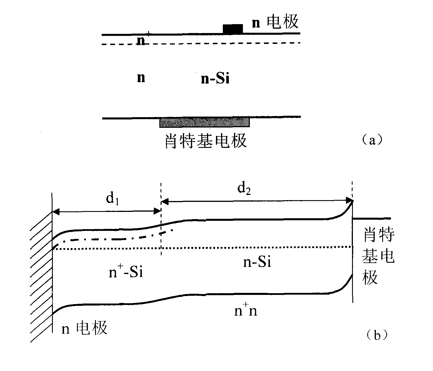
The invention discloses a method for preparing a silicon detector with high photoelectric response at the room temperature. The method is characterized by comprising the following steps of: preparing a heavily doped n-type silicon (Si) layer with an impurity deep energy level on a light receiving surface of an n-type Si substrate, preparing a transparent conductive film on the heavily doped n-type Si layer, and preparing an ohmic contact n electrode on the transparent conductive film serving as a first electrode; and preparing a Schottky electrode on a back surface or the light receiving surface of the n-type Si substrate serving as a second electrode, or forming a p-type Si region on the back surface or the light receiving surface of the n-type Si substrate, and preparing an ohmic contact p electrode on the p-type Si region serving as the second electrode. By using the method, the photoelectric response of the silicon detector can be greatly improved, namely the flexibility is improved and the detection range is expanded to an infrared light region.

Description

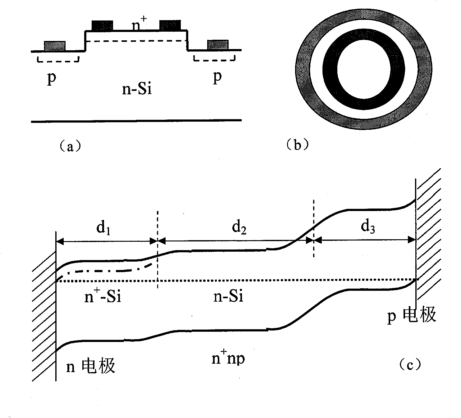
Technical field [0001] Background technique [0002] [1] Essence [0003] [2] Essence [0004] [1] [2] Essence [0005] [3] Essence [0006] [0007] references: [0008] [0009] [0010] Invention content [0011] (1) Technical problems to be solved [0012] [0013] [0014] [0015] [0016] [0017] [0018] [0019] [0020] [0021] [0022] [0023] [0024] [0025] [0026] [0027] [0028] [0029] [0030] [0031] [0032] [0033] [0034] [0035] [0036] [0037] [0038] [0039] [0040] [0041] [0042] [0043] [0044] Attachment description [0045] figure 1 [0046] figure 2 [0047] image 3 [0048] Figure 4The first and second electrodes prepared by the present invention are on the Si substrate to welcomes the light, and the second electrode of the second electrode of the highlights of the silicon detector of the silicon detector (A) and the overwhelming view (b), andThe device structure can bring graph (C). [0049] Figure 5 The first and se...

Claims


Application Information

Patent Timeline
IPC IPC(8): H01L31/18
CPCY02P70/50
Inventor 韩培德
Owner INST OF SEMICONDUCTORS - CHINESE ACAD OF SCI
Learn More