Self-aligned T-gate carbon nanotube field effect transistor devices and method for forming the same

A technology of field effect transistors and nanotubes, applied in the field of nanotube field effect transistors, can solve the problems of CNT integrated FET difficulties, large-scale manufacturing of consistent characteristics and uniform characteristics, etc.

Inactive Publication Date: 2010-11-24
RF NANO
View PDF0 Cites 11 Cited by
  • Summary
  • Abstract
  • Description
  • Claims
  • Application Information

AI Technical Summary

Problems solved by technology

As the process geometries for FETs continue to decrease, it becomes increasingly more difficult to manufacture FETs at scale, to have consis

Method used


Image

  • Self-aligned T-gate carbon nanotube field effect transistor devices and method for forming the same
  • Self-aligned T-gate carbon nanotube field effect transistor devices and method for forming the same
  • Self-aligned T-gate carbon nanotube field effect transistor devices and method for forming the same

Examples


Embodiment Construction

[0009] Detailed description of the preferred embodiment

[0010] The present invention is directed to self-aligned T-gate carbon nanotube (CNT) field effect transistors (FETs) and methods for forming the devices.

[0011] In one or more embodiments described herein, for each description, while nanotubes may be described as layers of carbon nanotubes, it should be understood that the nanotubes may include any type of nanotube, including but not limited to carbon nanotubes. tubes, single-walled nanotubes (SWNTs) and multi-walled nanotubes (MWNTs). Furthermore, each of the various embodiments may also be implemented in any one-dimensional semiconductor device (eg, nanotube, nanowire, etc.) or two-dimensional semiconductor device (eg, graphene-based device, etc.).

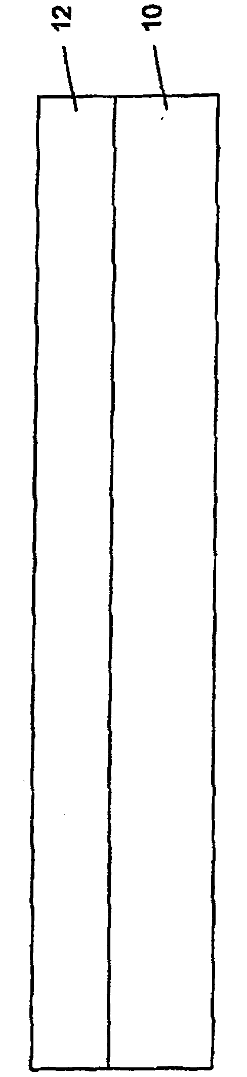
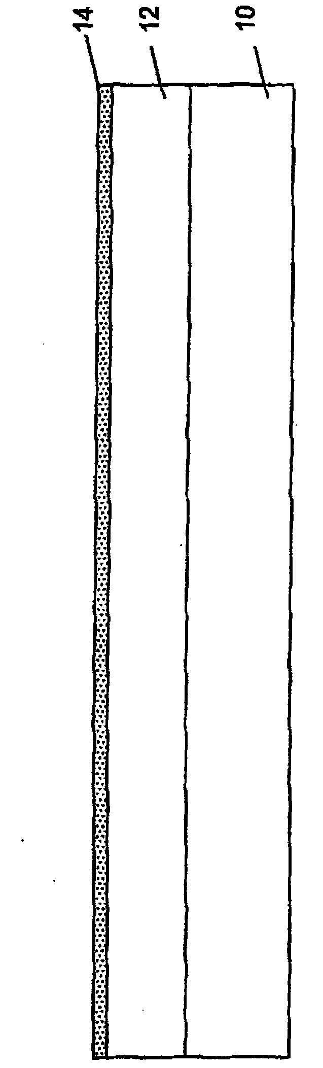
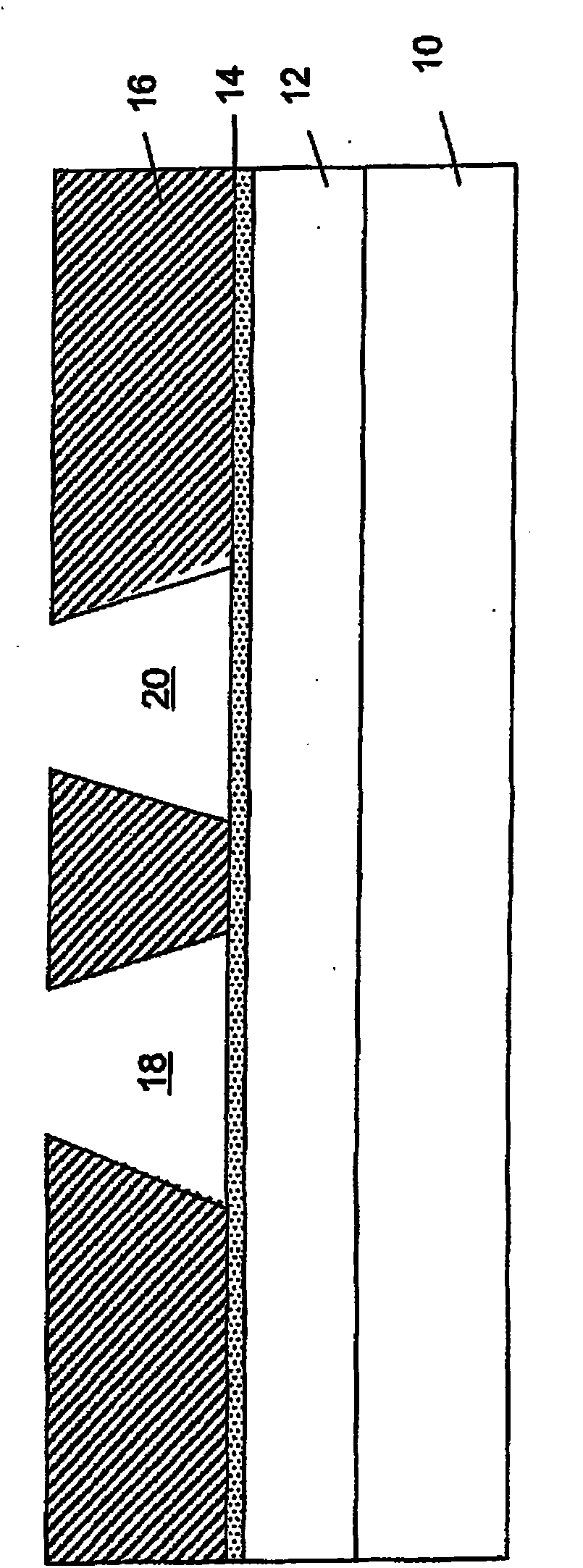
[0012] According to one or more embodiments, a method for forming a self-aligned T-gate carbon nanotube field effect transistor is provided. now refer to Figures 1 to 8 , various process steps for forming a CNT FET...


PUM


Abstract

A method is provided for forming a self-aligned carbon nanotube (CNT) field effect transistor (FET). According to one feature, a self-aligned source-gate-drain (S-G-D) structure is formed that allows for the shrinking of the gate length to arbitrarily small values, thereby enabling ultra-high performance CNT FETs. In accordance with another feature, an improved design of the gate to possess a ''T''-shape, referred to as the ''T-Gate,'' thereby enabling a reduction in gate resistance and further providing an increased power gain. The self-aligned T-gate CNT FET is formed using simple fabrication steps to ensure a low cost, high yield process.

Description

[0001] This application claims the benefit of and priority to US Provisional Application Serial No. 60 / 952,966, filed July 31, 2007, the contents of which are incorporated herein by reference in their entirety. technical field [0002] The present invention relates to nanotube (NT) field effect transistors (FETs), and more particularly, to self-aligned T-gate carbon nanotube field effect transistors (CNT FETs). Background technique [0003] One of the challenges facing the widespread commercialization of nanotube technology is the lack of a clear path for integrating carbon nanotubes (CNTs) with field effect transistors. As the process geometries for FETs continue to decrease, it becomes increasingly more difficult to manufacture FETs at scale, to have consistent and uniform characteristics across all FETs, and to even integrate CNTs into FETs of this reduced scale It is also increasingly difficult. Contents of the invention [0004] According to one or more embodiments, ...

Claims


Application Information

Patent Timeline
IPC IPC(8): H01L21/336
CPCB82Y10/00H01L29/78684H01L29/0665H01L51/055H01L29/1606H01L51/0541H01L51/0048H01L29/42384H01L29/7781H01L29/0673H10K85/221H10K10/481H10K10/464
Inventor A·M·卡尔伯格
Owner RF NANO
Why Eureka
Try Eureka