Thin-film solar cell

A solar cell and thin film technology, applied in circuits, photovoltaic power generation, electrical components, etc., can solve problems such as unreasonable design of solar cell modules, and achieve the effects of reasonable thickness, increased power, and increased power.

Inactive Publication Date: 2010-12-01
河南阿格斯新能源有限公司
View PDF2 Cites 10 Cited by
  • Summary
  • Abstract
  • Description
  • Claims
  • Application Information

AI Technical Summary

Problems solved by technology

However, the module design of the existing a-Si / CIGS series multi-junction solar cells is not reasonable enough, and its current photoelectric conversion efficiency is only about 10%.

Method used


Image

  • Thin-film solar cell
  • Thin-film solar cell
  • Thin-film solar cell

Examples


Embodiment 1

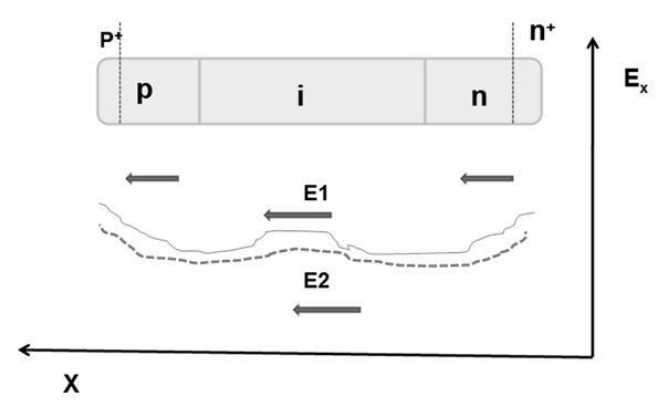
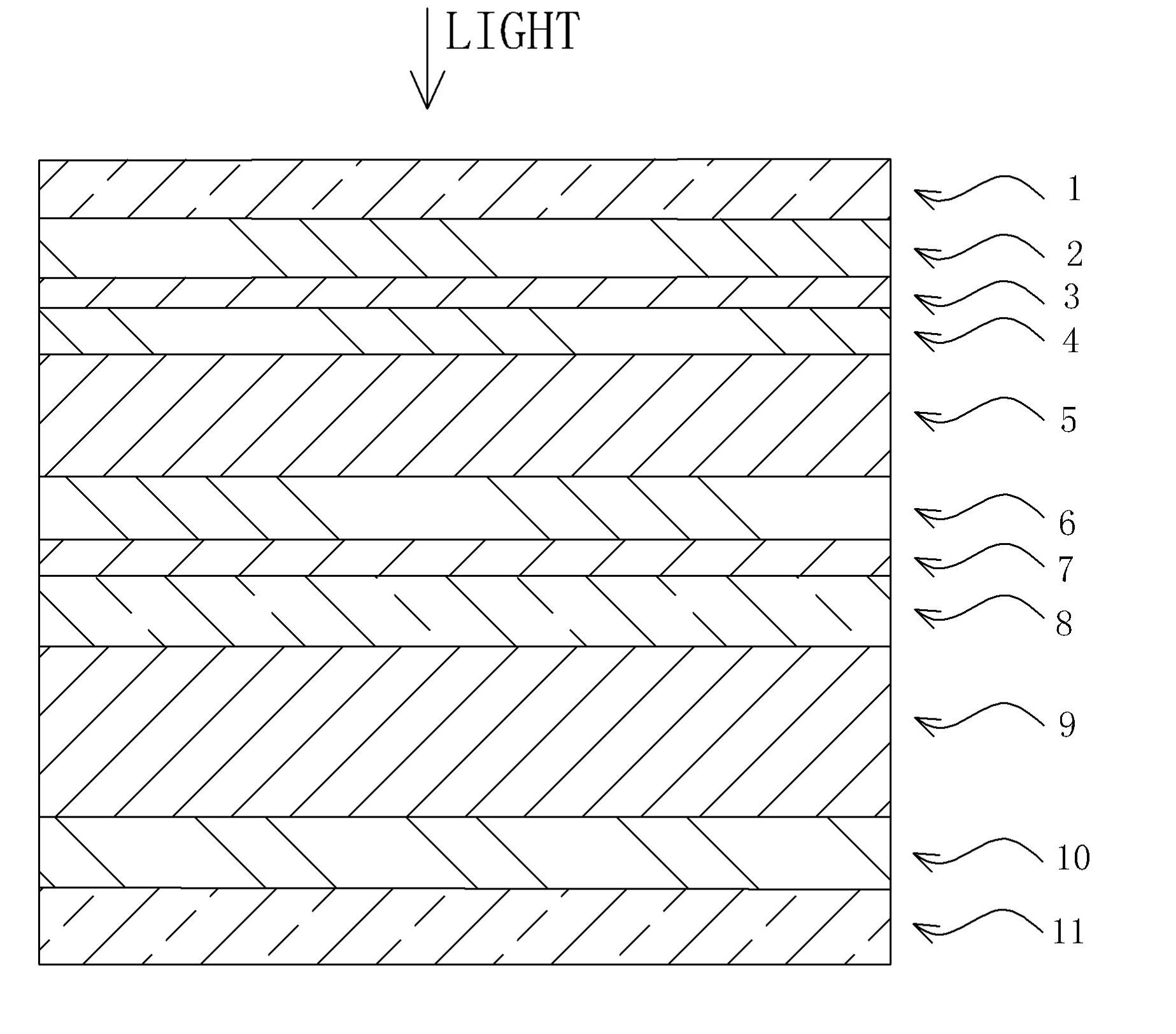
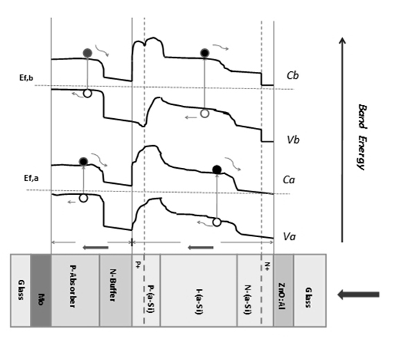
[0020] like figure 2 As shown, the thin-film solar cell of an embodiment of the present invention has a structure of: glass substrate layer 11 / Mo back electrode layer 10 / P-type copper indium gallium selenide thin film layer 9 / N-type copper indium gallium selenide buffer layer 8 / P + Layer 7 / P-type amorphous silicon layer 6 / I-type amorphous silicon layer 5 / N-type amorphous silicon layer 4 / N + Layer 3 / ZnO:Al layer 2 / front glass lining layer 1, sunlight enters from the front glass lining layer 1, and passes through ZnO:Al layer 2, N + Layer 3, N-type amorphous silicon layer 4, I-type amorphous silicon layer 5, P-type amorphous silicon layer 6, P + Layer 7 and N-type CIGS buffer layer 8 are then completely absorbed by P-type CIGS thin film layer 9 .

[0021] Among them, the thickness of the amorphous silicon P-I-N junction layer is 100nm, and the thickness ratio of the P-type amorphous silicon layer 6, the I-type amorphous silicon layer 5 and the N-type amorphous silicon layer ...

Embodiment 2

[0023] The structure of the thin film solar cell of this embodiment is the same as the structure of the thin film solar cell of Embodiment 1, see the structure figure 2 As shown, its structure is: glass substrate layer 11 / Mo back electrode layer 10 / P-type copper indium gallium selenide thin film layer 9 / N-type copper indium gallium selenide buffer layer 8 / P + Layer 7 / P-type amorphous silicon layer 6 / I-type amorphous silicon layer 5 / N-type amorphous silicon layer 4 / N + Layer 3 / ZnO:Al layer 2 / front glass lining layer 1, sunlight enters from the front glass lining layer 1, and passes through ZnO:Al layer 2, N + Layer 3, N-type amorphous silicon layer 4, I-type amorphous silicon layer 5, P-type amorphous silicon layer 6, P + Layer 7 and N-type CIGS buffer layer 8 are then completely absorbed by P-type CIGS thin film layer 9 .

[0024] The difference is: the thickness of the amorphous silicon P-I-N junction layer is 360nm, and the thickness ratio of the P-type amorphous silicon ...

Embodiment 3

[0026] The structure of the thin film solar cell of this embodiment is the same as the structure of the thin film solar cell of Embodiment 1, see the structure figure 2 As shown, its structure is: glass substrate layer 11 / Mo back electrode layer 10 / P-type copper indium gallium selenide thin film layer 9 / N-type copper indium gallium selenide buffer layer 8 / P + Layer 7 / P-type amorphous silicon layer 6 / I-type amorphous silicon layer 5 / N-type amorphous silicon layer 4 / N + Layer 3 / ZnO:Al layer 2 / front glass lining layer 1, sunlight enters from the front glass lining layer 1, and passes through ZnO:Al layer 2, N + Layer 3, N-type amorphous silicon layer 4, I-type amorphous silicon layer 5, P-type amorphous silicon layer 6, P + Layer 7 and N-type CIGS buffer layer 8 are then completely absorbed by P-type CIGS thin film layer 9 .

[0027] The difference is: the thickness of the amorphous silicon P-I-N junction layer is 200nm, and the thickness ratio of the P-type amorphous silicon ...


PUM


Abstract

The invention discloses a thin-film solar cell structurally comprising a substrate layer, a back electrode layer, a P-type CIGS (copper, indium, gallium and selenium) thin-film layer, an N-type CIGS cushion layer, a P+ layer, a P-type a-Si (amorphous silicon) layer, an I-type a-Si layer, an N-type a-Si layer, an N+ layer and an TCO (transparent conducting oxide) layer. The thin-film solar cell of the invention is an a-Si P-I-N junction layer has reasonable thickness design and the NIR (near infrared spectrum) energy can be completely absorbed by a CIGS P-N junction layer, thus greatly increasing the power of the thin-film solar cell; moreover, the P+ layer and the N+ layer which are ultrathin but heavily doped are respectively arranged outside the P-type a-Si layer and the N-type a-Si layer of the a-Si P-I-N junction layer, thus increasing the electric-field intensity of the I-type a-Si layer and increasing the power of the thin-film solar cell. Compared with the existing double-junction-layer structured solar cells of the same type, the thin-film solar cell of the invention can increase the power thereof by about 1.5% on average. The thin-film solar cell of the invention further has the advantages of high reliability and low manufacturing cost.

Description

technical field [0001] The invention belongs to the technical field of photovoltaic solar cells, and in particular relates to a thin-film solar cell. Background technique [0002] CIGS is the abbreviation of copper indium gallium selenide solar cell. The tandem cell composed of CIGS and a-Si thin film cells has attracted great attention from the beginning due to its advantages of high efficiency, low attenuation rate, easy operation and improvement of the production process. big concern. In U.S. Patent Publication No. 6368892, a multi-junction solar cell composed of CIGS and a-Si thin film cells connected in series is disclosed. Its structure is: substrate layer / back electrode layer / CIS (or CIGS) layer / n-type conductive layer / P-I-N junction layer / front electrode layer. However, the module design of the existing a-Si / CIGS tandem multi-junction solar cells is not reasonable enough, and its current photoelectric conversion efficiency is only about 10%. Contents of the inve...

Claims


Application Information

Patent Timeline
Patent Type & Authority Applications(China)
IPC IPC(8): H01L31/042H01L31/0352H01L31/0445
CPCY02E10/50
Inventor 赵一辉贺方涓
Owner 河南阿格斯新能源有限公司
Why Eureka
Try Eureka