Method and device for comprehensively recycling waste printed circuit boards

A circuit board and waste printing technology, applied in the field of environmental engineering, can solve the problem of low comprehensive utilization rate of the treatment method, and achieve the effects of simple structure, easy enlargement and strong process adaptability

Active Publication Date: 2010-12-08
GUANGZHOU INST OF ENERGY CONVERSION - CHINESE ACAD OF SCI
View PDF7 Cites 17 Cited by
  • Summary
  • Abstract
  • Description
  • Claims
  • Application Information

AI Technical Summary

Problems solved by technology

[0006] The purpose of the present invention is to overcome the technical problem of low comprehensive utilization rate of waste printed circuit board treatment methods in the prior art, and provide a method based on the principle of thermochemical conversion, which combines gasification and bromide removal, and makes full use of waste printed circuit boards. Energy resources in boards, recycling inorganic fillers and precious metals such as copper and aluminum, and realizing efficient and low-pollution comprehensive treatment methods and devices for waste printed circuit boards

Method used


Image

  • Method and device for comprehensively recycling waste printed circuit boards
  • Method and device for comprehensively recycling waste printed circuit boards
  • Method and device for comprehensively recycling waste printed circuit boards

Examples


Embodiment 1

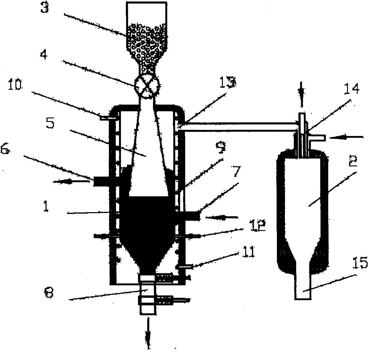
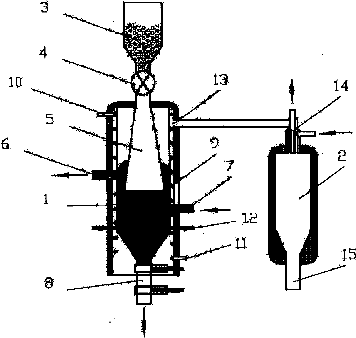
[0024] A method for comprehensive recycling of waste printed circuit boards, comprising the following steps:

[0025] (1) Gasification of waste printed circuit boards: the waste printed circuit boards enter the molten salt reaction furnace after being crushed. The molten salt is a binary salt, which includes 71% Na 2 CO 3 and 29%K 2 CO 3 , gasification at 700-900°C to obtain gasification residues and gas products containing a large amount of tar. The gasification residues are stratified in the molten salt, and are discharged from the molten salt reaction furnace from different positions of the molten salt reaction furnace for recycling respectively;

[0026](2) Removal of bromine-containing pollutants: when waste printed circuit boards are gasified in molten salt, Br in waste printed circuit boards is mainly released in the form of HBr, and the released acidic HBr is immediately absorbed by alkaline molten salt, At the same time, a small amount of bromine-containing organic...

Embodiment 2

[0039] The molten salt in the molten salt reaction furnace of this embodiment is a ternary salt, which consists of the following components:

[0040] 39% Li 2 CO 3 -38.5%K 2 CO 3 -22.5% Rb 2 CO 3 ;

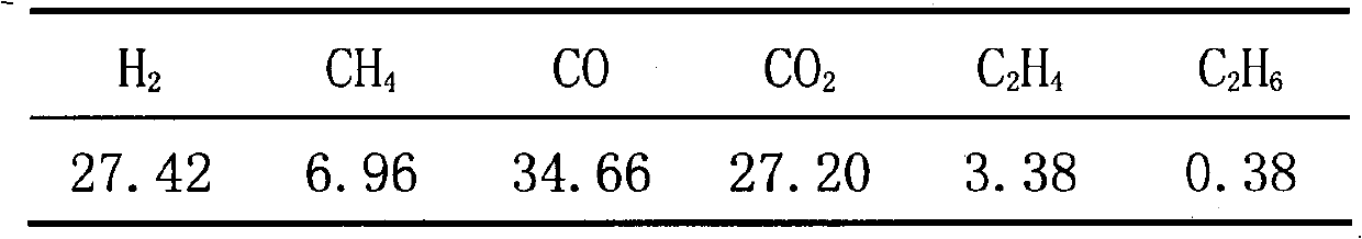
[0041] The gas volume ratio of oxygen-enriched air, gaseous product, and water vapor is=1:0.6:1; get H at the same time 2 Syngas / CO ratio of 0.9.

[0042] Other structures of this embodiment are the same as those of Embodiment 1, and will not be described in detail here.

Embodiment 3

[0044] The molten salt in the molten salt reaction furnace of this embodiment is a ternary salt, which consists of the following components:

[0045] 43.5% Li 2 CO 3 -31.5% Na 2 CO 3 -25%K 2 CO 3 ;

[0046] The gas volume ratio of oxygen-enriched air, gaseous product, and water vapor is=1:0.7:3; simultaneously obtain H 2 Syngas / CO ratio of 1.2.


PUM


Abstract

The invention discloses a method for comprehensively recycling waste printed circuit boards, which comprises the following: a step of waste printed circuit board gasification, which is to crush the waste printed circuit boards, feed the crushed waste printed circuit boards into a molten salt reacting furnace, perform gasification at the temperature of between 700 and 900 DEG C to obtain gasified residues and a gas product which contains a large amount of tar, allow the gasified residues to layer in molten salt, discharge the layered products from different positions of the molten salt reacting furnace and recycle the products respectively; a step of bromine-containing pollutant removal, which is to release bromine (Br) from the waste printed circuit boards in a form of hydrogen bromide (HBr) when the waste printed circuit boards are gasified, wherein the released acid HBr is instantly absorbed by alkali molten salt and a small amount of bromine-containing organic materials generated at the same time are cracked and absorbed by the molten salt under the catalysis of the molten salt; and a step of gas product reforming, which is to introduce the mixture of the gas product containing a large amount of tar, oxygen-enriched air and vapor according to a ratio of 1: (0.4-0.7): (1-5) into an airflow bed, reform at the temperature of between 1,200 and 1,500 DEG C, regulate the ratio of hydrogen (H2) to carbon monoxide (CO) in the gas to 0.8 to 2 and convert the tar in the gas product at a high temperature in the airflow bed.

Description

technical field [0001] The invention relates to the technical field of environmental engineering, in particular to a device and method for energy utilization of printed circuit boards and recycling of inorganic fillers and metals such as copper and aluminum in the circuit boards. Background technique [0002] Waste printed circuit board (Printed circuit board, PCB) is the basis of the electronics industry, widely used in computers and components, communication equipment, measurement and control instruments, household electronic appliances and other fields. Due to the rapid replacement of products in the electronics and information industries, the amount of waste printed circuit boards produced is also very alarming. In recent years, the average growth rate of waste printed circuit boards in the world has reached 8.7%, and the annual growth rate in Southeast Asia is 10.8%, while the growth rate in my country is as high as 14.4%. In 2006, the output value of waste printed circ...

Claims


Application Information

Patent Timeline
Patent Type & Authority Applications(China)
IPC IPC(8): B09B3/00
CPCY02W30/82
Inventor 赵增立王小波李海滨
Owner GUANGZHOU INST OF ENERGY CONVERSION - CHINESE ACAD OF SCI
Why Eureka
Try Eureka