Surface cleaning method on indium antimonide wafer after alkaline chemical mechanical polishing

An indium antimonide wafer and chemical mechanical technology, which is applied in the field of surface cleaning of semiconductor indium antimonide wafers after alkaline chemical mechanical polishing, can solve the problems of uneven corrosion on the surface of indium antimonide materials, lower device yields, and high wafer surface temperatures, etc. problems, to achieve the effect of preventing local continuous reaction, good temperature consistency and consistent temperature distribution

Inactive Publication Date: 2010-12-15
HEBEI UNIV OF TECH
View PDF6 Cites 3 Cited by
  • Summary
  • Abstract
  • Description
  • Claims
  • Application Information

AI Technical Summary

Problems solved by technology

[0003] At present, after mass polishing of indium antimonide materials, the surface is cleaned by washing with water. Due to the high temperature, high energy, and high surface tension of the wafer surface, although the polishing has stopped, the reaction on the wafer surface has a lagging process. Simple Rinsing with water cannot avoid the phenomenon of uneven distribution of polishing liquid, contamination of metal ions, etc., resulting in uneven corrosion on the surface of the cleaned indium antimonide material, increased roughness, and corrosion rings on the surface of the cleaned indium antimonide material. On an 8-inch chip, there are more than 1,000 particles with a particle size larger than 0.1 micron, which will increase the cost in subsequent processing and reduce the yield of the device

Method used


Image

  • Surface cleaning method on indium antimonide wafer after alkaline chemical mechanical polishing

Examples


Embodiment 1

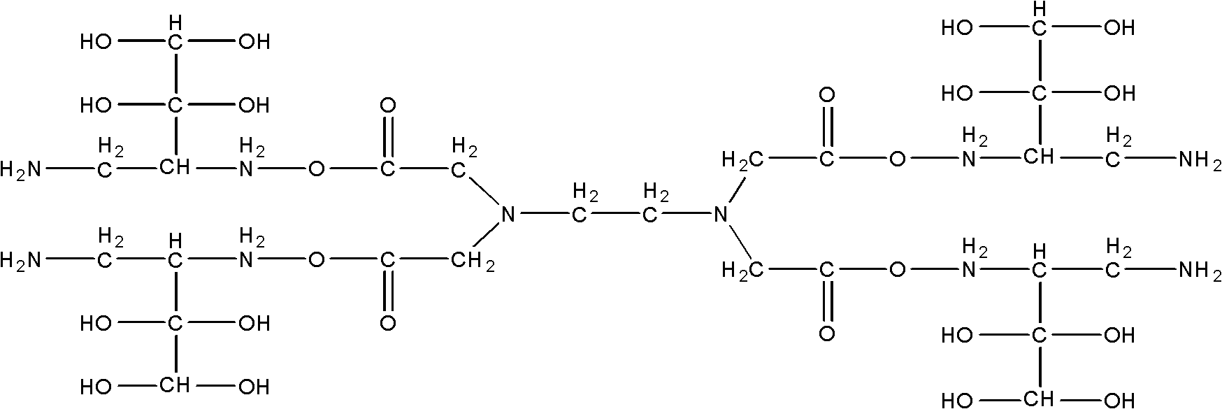
[0025] (1) Take 497g of ultrapure water with a resistance of 18MΩ, add 2.5g of FA / OI type surfactant and 0.5g of FA / O II type chelating agent while stirring, and get a pH value of 6.7 after stirring evenly, which is approximately neutral Water-soluble surface cleaner.

[0026] (2) The semiconductor indium antimonide wafer after alkaline chemical mechanical polishing is quickly polished and cleaned for 30 s with the cleaning solution obtained in step (1) at a flow rate of 1000 ml / min and a pressure of its own weight.

[0027] (3) be 18MΩ ultrapure water 499.5g to dilute corrosion inhibitor benzotriazole 0.5g with resistance, be 1000ml to the indium antimonide wafer after step (2) cleaning rapidly with the benzotriazole solution after dilution / min, polishing and cleaning for 30s under the condition of self-weight pressure.

[0028] (4) Rinse the indium antimonide wafer cleaned in step (3) for 30 seconds with ultrapure water with a resistance of 18 MΩ under the conditions of ze...

Embodiment 2

[0031] (1) get the ultrapure water 2054g that resistance is 18MΩ, add surfactant O while stirring π -10 42g and 38g of FA / O II type chelating agent, after stirring evenly, the pH value is 6.9 and is approximately neutral water-soluble surface cleaning solution.

[0032] (2) The semiconductor indium antimonide wafer after alkaline chemical mechanical polishing was quickly polished and cleaned for 80 seconds with the cleaning solution obtained in step (1) at a flow rate of 1600 ml / min and a pressure of 0.01 atmosphere.

[0033] (3) be the ultrapure water 2096g dilution hexamethylenetetramine corrosion inhibitor 38g of 18M Ω with resistance, quickly to the indium antimonide wafer after step (2) cleaning at zero with the hexamethylenetetramine solution after dilution Polishing and cleaning for 80s under the conditions of pressure (self-weight pressure) and flow rate of 1600ml / min.

[0034] (4) Rinse the indium antimonide wafer cleaned in step (3) for 80 seconds with ultrapure wat...

Embodiment 3

[0037](1) Take 5643.56g of ultrapure water with a resistance of 18MΩ, add 12.42g of surfactant O-202 and 212.42g of FA / O II type chelating agent while stirring, and get a pH value of 7.3 after stirring evenly, which is approximately neutral. Non-toxic surface cleaner.

[0038] (2) Quickly use the cleaning liquid obtained in step (1) to polish and clean the semiconductor indium antimonide wafer after alkaline chemical mechanical polishing for 130 seconds under the conditions of a flow rate of 2800 ml / min and a pressure of 0.005 atmospheres.

[0039] (3) Dilute the benzotriazole corrosion inhibitor 212.42g with the ultrapure water 5855.98g of 18MΩ with resistance, carry out the indium antimonide wafer after step (2) cleaning rapidly with the flow rate of benzotriazole solution after dilution Polishing and cleaning for 130s under the conditions of 2800ml / min and zero pressure (self-weight pressure).

[0040] (4) Using ultrapure water with a resistance of 18 MΩ at zero pressure (...


PUM

PropertyMeasurementUnit
Surface roughnessaaaaaaaaaa

Abstract

The invention discloses a surface cleaning method on indium antimonide wafer after alkaline chemical mechanical polishing. The invention aims at providing a method which can reduce downstream processing cost of indium antimonide wafer after alkaline chemical mechanical polishing, is simple and easy and can improve surface evenness and cleanliness of wafer. Ultrapure water with the resistance of more than 18Mohm is subject to stirring while surfactant and FA / O II chelating agent are added, stirring to be uniform is carried out, so as to obtain clean solution; the clean solution is adopted to rapidly carry out polishing cleaning on indium antimonide wafer after alkaline chemical mechanical polishing for at least 30s under the conditions of high flow of 1000-5000ml / min and low pressure of 0-0.0 atmospheric pressure; ultrapure water with the resistance of more than 18Mohm is adopted to dilute corrosion inhibitor, and high flow polishing cleaning is carried out on indium antimonide wafer after cleaning for at least 30s under the condition of zero pressure; and finally ultrapure water with the resistance of more than 18Mohm is adopted to wash the indium antimonide wafer after cleaning for at least 30s under the conditions of zero pressure and high flow.

Description

technical field [0001] The invention belongs to the cleaning technology of the wafer surface, and more specifically relates to a method for cleaning the surface of a semiconductor indium antimonide wafer after alkaline chemical mechanical polishing. Background technique [0002] The InSb staring infrared focal plane device with a response in the 1-5.5 μm band has the advantages of high sensitivity, mature technology, and good cost-effectiveness. At present, it occupies a dominant position in the field of military staring infrared. Examples include the US ballistic missile defense system and several critical conventional tactical weapons systems. InSb focal plane devices are widely used in guidance and thermal imaging devices. In terms of civil use, InSb thermal imaging technology is widely used in medical diagnosis, fire protection, rescue, industrial monitoring, forest protection and other fields. In air-to-air imaging guidance applications, the 64×64 element InSb starin...

Claims


Application Information

Patent Timeline
IPC IPC(8): B08B3/10B08B3/08
Inventor 刘玉岭王娟李晖
Owner HEBEI UNIV OF TECH
Why Eureka
Try Eureka