LDMOS device with multilayer super-junction structure

A device and active region technology, which is applied in semiconductor devices, semiconductor/solid-state device manufacturing, electrical components, etc., can solve problems such as device damage, reduced breakdown resistance, and uneven distribution of impurities in the column area, so as to improve the contact area, The effect of high resistance to breakdown

Inactive Publication Date: 2010-12-15
SHANGHAI INST OF MICROSYSTEM & INFORMATION TECH CHINESE ACAD OF SCI +1
View PDF5 Cites 13 Cited by
  • Summary
  • Abstract
  • Description
  • Claims
  • Application Information

AI Technical Summary

Problems solved by technology

[0005] Usually, in order to make devices with the same drift region length and width fully depleted as much as possible under the maximum breakdown voltage, the width of the p / n column area can be reduced and the depth of the p / n column area can be increased, that is, the column area can be increased as much as possible. The essence of the aspect ratio of the region is to increase the contact area between the p / n column regions, that is, to increase the area of ​​the p / n junction depletion region inside the drift region. However, it is actually limited by the process conditions and cannot Further obtain a smaller pillar region width and a deeper pillar region depth, which is because: firstly, superjunction devices need to be annealed in the subsequent high-energy ion implantation process, so narrow pillar regions are likely to cause different types of Impurities diffuse and pollute each other, resulting in an imbalance of charges inside the p / n column region, which will reduce the actual breakdown resistance; secondly, too deep a column region is bound to be accompanied by high-energy ion implantation, which is likely to cause internal damage to the device, and the column region The distribution of internal impurities is very uneven, which will still cause the problem of charge imbalance between adjacent p / n columns, thereby reducing the actual breakdown resistance of the device

Method used


Image

  • LDMOS device with multilayer super-junction structure
  • LDMOS device with multilayer super-junction structure
  • LDMOS device with multilayer super-junction structure

Examples


Embodiment Construction

[0038] The present invention will be further described below in conjunction with the accompanying drawings, which are not drawn to scale for the convenience of illustration.

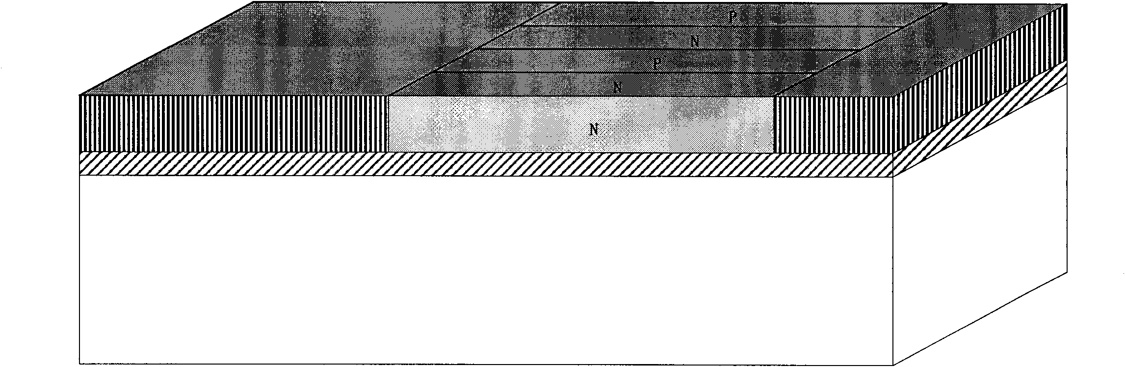
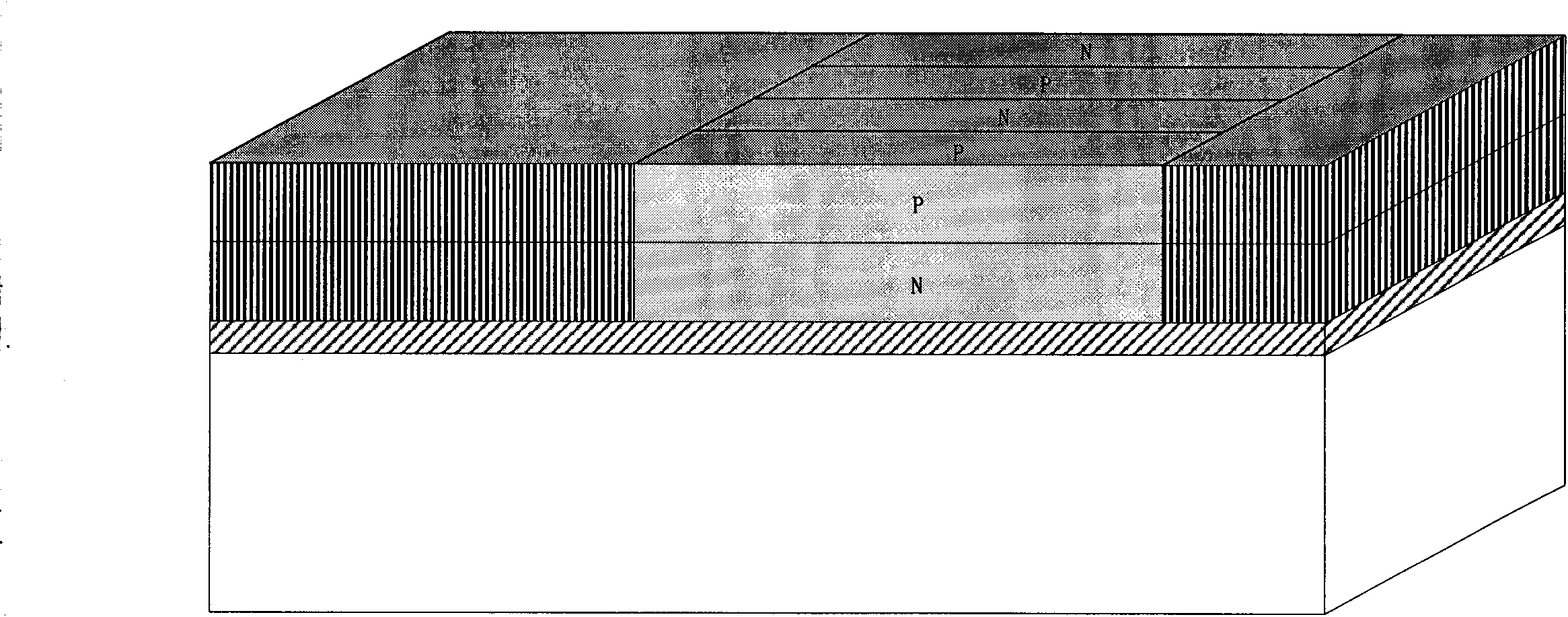
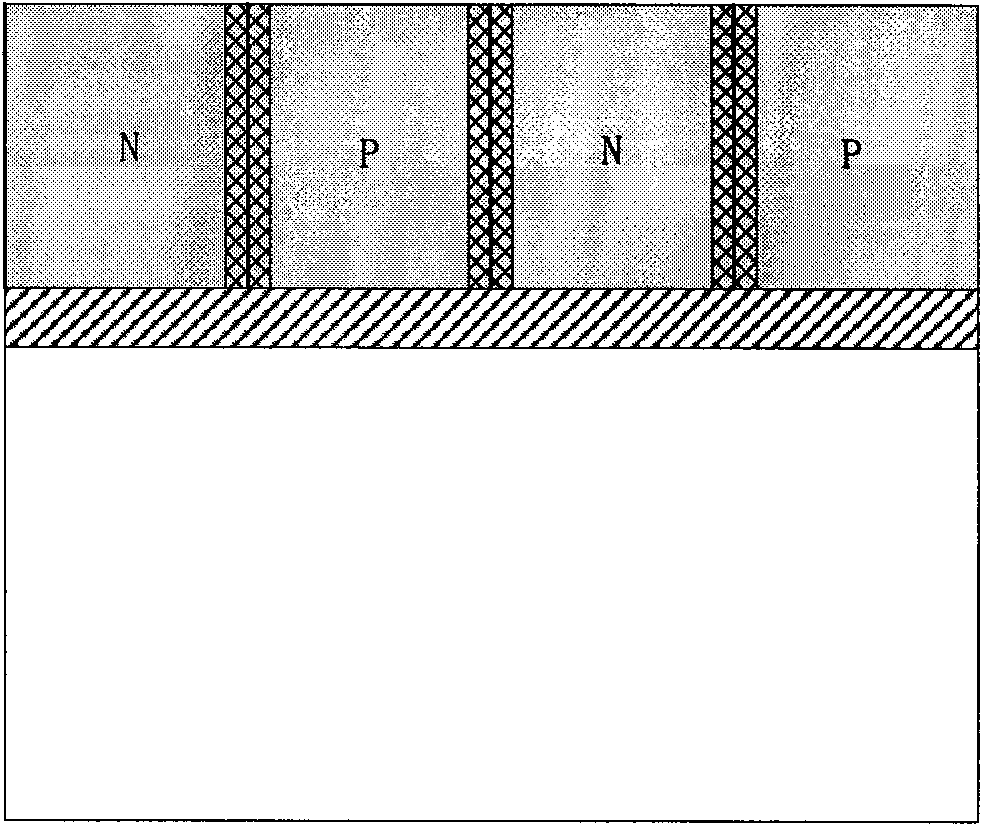
[0039] Such as Figure 5 As shown, an LDMOS device with a multilayer superjunction structure includes a substrate and an active region on the substrate, and its active region includes: a gate region, a source region 11 and a drain region on both sides of the gate region 16. A body region 12 located under the gate region, a multilayer super junction structure located between the body region 12 and the drain region 16; the multilayer super junction structure includes at least two layers of super junction structures ( Including the first layer of super junction structure 14 and the second layer of super junction structure 15), each layer of super junction structure is composed of n-type pillar regions 5 and p-type pillar regions 4 alternately arranged laterally, which can share the breakdown voltage. Where...


PUM


Abstract

The invention discloses an LDMOS device with a multilayer super-junction structure. An active region of the device comprises a grid region, a source region and a drain region positioned on two sides of the grid region, a body region positioned under the grid region, and the multilayer super-junction structure positioned between the body region and the drain region, wherein the multilayer super-junction structure comprises at least two layers of super-junction structures arranged from bottom to top in turn; each layer of super-junction structure consists of n-type columnar regions and p-type columnar regions which are transversely and alternately arranged, preferably, the n-type columnar regions and the p-type columnar regions of upper and lower layers of super-junction structures are alternately arranged. The multilayer super-junction structure of the device can further improve the contact area among the n-type columnar regions and the p-type columnar regions, and simultaneously a method for manufacturing the structure cannot bring obvious side effects, so the anti-breakdown capacity of the device can be ensured to be higher than that of the conventional super-junction LDMOS device, and the multilayer super-junction structure also has high expansibility.

Description

technical field [0001] The invention relates to a lateral double-diffused metal oxide semiconductor (LDMOS, Lateral Double-diffused MOSFET), in particular to an LDMOS device with a multilayer superjunction structure, belonging to the technical field of semiconductor manufacturing. Background technique [0002] Lateral Double-diffused MOSFET (LDMOS, Lateral Double-diffused MOSFET) is the key technology of high-voltage integrated circuit HVIC (High Voltage Integrated Circuit) and power integrated circuit PIC (Power Integrated Circuit). Its main feature is that a relatively long lightly doped drift region is added between the channel region and the drain region. The doping type of the drift region is consistent with that of the drain end. By adding the drift region, it can share the breakdown voltage. [0003] The so-called super-junction LDMOS is an improved LDMOS, that is, the low-doped N-type drift region of the traditional LDMOST is replaced by a set of alternately arranged...

Claims


Application Information

Patent Timeline
Patent Type & Authority Applications(China)
IPC IPC(8): H01L29/78H01L29/06H01L21/336
CPCH01L29/7824H01L29/0634
Inventor 程新红何大伟王中健徐大伟宋朝瑞俞跃辉
Owner SHANGHAI INST OF MICROSYSTEM & INFORMATION TECH CHINESE ACAD OF SCI
Why Eureka
Try Eureka