FPGA (Field Programmable Gate Array)-based bonded phase frequency doubling method and device

A key-phase and frequency multiplication technology, applied to logic circuits using basic logic circuit components, logic circuits using specific components, electrical components, etc., can solve the problem of multi-circuit area, inability to perform period prediction and error correction, and inability to adapt to distribution Miniaturization and other issues to achieve the effect of improving stability and reliability, reducing circuit consumption area, flexible and convenient modification

Active Publication Date: 2010-12-15
ZHEJIANG UNIV
View PDF2 Cites 5 Cited by
  • Summary
  • Abstract
  • Description
  • Claims
  • Application Information

AI Technical Summary

Problems solved by technology

At present, it is generally implemented by a group of separate functional devices working together, so there are many components and large volumes, which cannot adapt to the trend of distributed miniaturization, such as "Steam Turbine Technology", Volume 45, Issue 1, February 2003, "A A new type of key phase signal processing circuit and its error analysis", using various digital discrete components including addition counters, frequency dividers with a frequency division factor of 64, and subtraction counters to realize the frequency multiplication circuit of key phase signals. The frequency circuit can reali

Method used


Image

  • FPGA (Field Programmable Gate Array)-based bonded phase frequency doubling method and device
  • FPGA (Field Programmable Gate Array)-based bonded phase frequency doubling method and device
  • FPGA (Field Programmable Gate Array)-based bonded phase frequency doubling method and device

Examples


Embodiment Construction

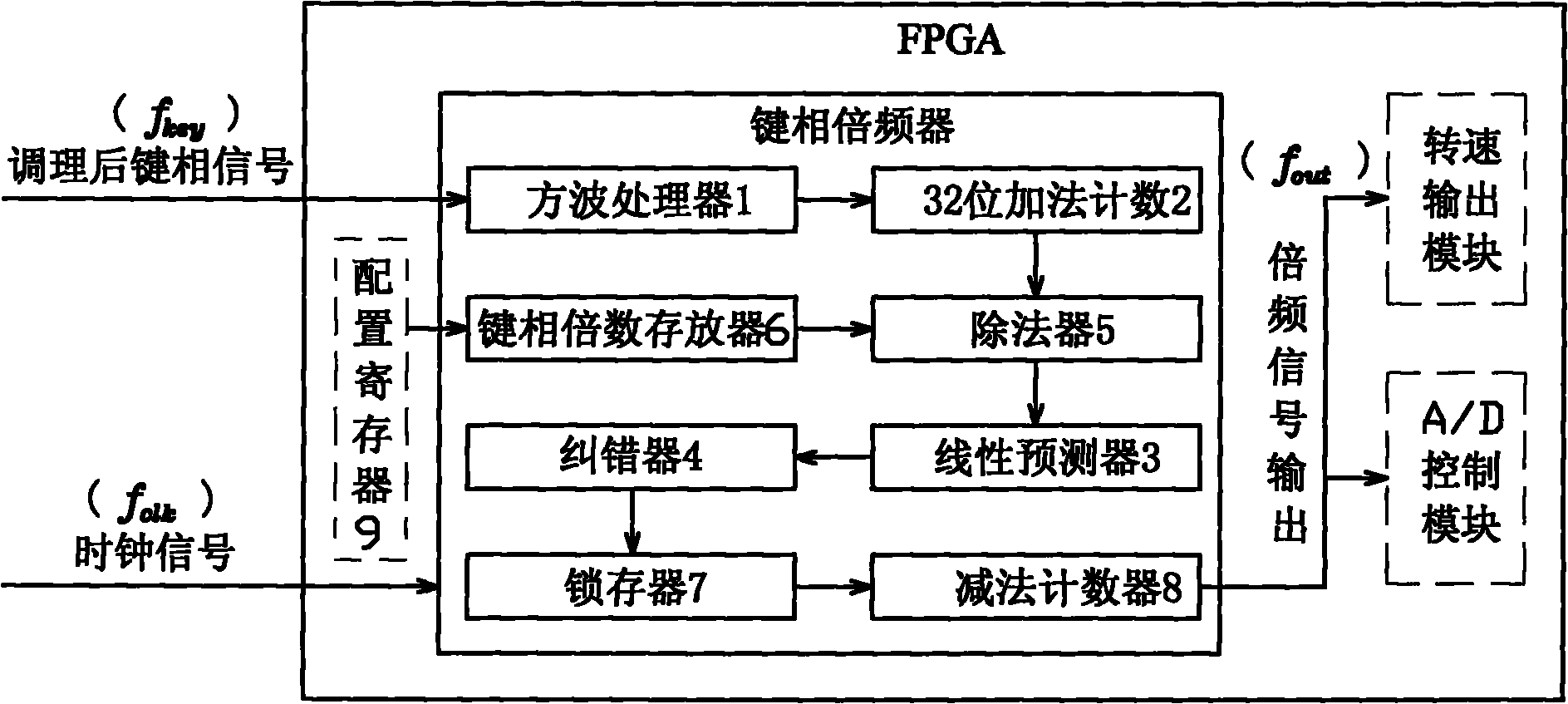
[0025] Such as figure 1 As shown, the FPGA-based key phase frequency multiplier of this embodiment includes a square wave processor 1, an addition counter 2, a linear predictor 3, an error corrector 4, a divider 5, a key phase multiple register 6, a latch Device 7 and subtraction counter 8, described square wave processor 1, addition counter 2, linear predictor 3, error corrector 4, divider 5, key phase multiple register 6, latch 7 and subtraction counter 8 use hardware The description language VHDL is programmed and integrated into an FPGA. The key-phase frequency multiplier is a module in the FPGA device, which accepts the frequency f key The key phase square wave signal, the clock signal and the data in the FPGA configuration register, wherein the key phase multiple 2 is placed in the FPGA configuration register 9 k (k is a positive integer) data, the device output frequency is 2 k f key The frequency multiplied square wave signal; the output multiplied signal can be us...


PUM


Abstract

The invention discloses FPGA (Field Programmable Gate Array)-based bonded phase frequency doubling method and device. The frequency doubling device comprises a square wave processor, an adding counter, a linear predicator, a corrector, a divider, a bonded phase multiple storage device, a latch and a subtract counter which are programmed by a VHDL (Visible Hardware Description Language) and are integrated into one FPGA. A bonded phase signal is processed by the square wave processor to become a standard square wave signal; the adding counter is used for counting the period of the square wave signal under the trigger of a clock signal; a counting value is transmitted to the linear predicator to predict a next periodical value of the bonded phase signal; a periodical predication value is checked by the corrector to be correct and then is transmitted to the divider for dividing by the bonded phase multiple to obtain a quotient which is latched by the latch; the subtract counter carries out the subtract counting by taking the quotient in the latch as a module value; and an overflow signal of the subtract counter is a frequency doubling signal. The device has compact structure; and the method and the device have the advantages of high integration degree, flexible configuration of frequency doubling coefficient, wide frequency doubling range, capability of periodical carrying out the linear detection on the bonded phase signal, high frequency doubling precision and higher stability and reliability.

Description

technical field [0001] The invention relates to the design of a Field Programmable Gates Array (Field Programmable Gates Array, FPGA), which is a method and a device for generating a key-phase frequency multiplication signal in the whole cycle sampling of the vibration signal of a rotating machine. Background technique [0002] There are a large number of large-scale rotating machinery and equipment in the process of electric power, petrochemical, and metallurgy. They are the foundation of the national economy. Once such machinery fails, it may cause a chain reaction, causing the entire machinery or even the entire set of equipment to fail to work normally, resulting in huge economic losses. It can even cause serious catastrophic casualties. In order to manage and use this kind of major key equipment well, improve the stability, reliability, safety, service efficiency and life of this kind of machinery, and avoid causing major accidents and affecting social production, the c...

Claims


Application Information

Patent Timeline
IPC IPC(8): H03B19/16H03K19/177
Inventor 杨世锡于保华梁文军
Owner ZHEJIANG UNIV
Why Eureka
Try Eureka