Field effect transistor chiral sensor and manufacture method thereof
What is AI technical title?
AI technical title is built by Patsnap AI team. It summarizes the technical point description of the patent document.
A field-effect transistor and sensor technology, applied in the field of sensors, can solve the problems of easy pollution and sensor application limitations, and achieve the effects of no reagent consumption, reduced environmental pollution, and easy deviceization
Inactive Publication Date: 2010-12-22
SUZHOU INST OF NANO TECH & NANO BIONICS CHINESE ACEDEMY OF SCI
View PDF6 Cites 22 Cited by
Summary
Abstract
Description
Claims
Application Information
AI Technical Summary
This helps you quickly interpret patents by identifying the three key elements:
Problems solved by technology
Method used
Benefits of technology
Problems solved by technology
However, when this method detects chiral molecules, the main substance and the chiral selective agent are combined in the liquid phase, and the main substance system to be tested is easily polluted. Generally, it can only be used once, and the application of the sensor is greatly limited.
Method used
Image
Click on the blue label to locate the original text in one second.
Reading with bidirectional positioning of images and text.
Examples
Embodiment 1
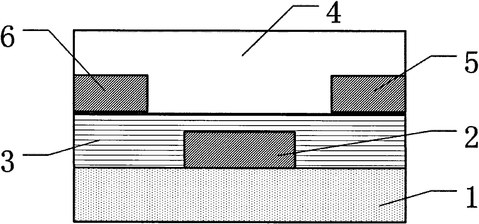
[0026] What is obtained by this preparation method is a top-contact quantum dot field effect transistor chiral sensor:
[0027] Step 1, sputtering or evaporating a layer of gate electrode 2 with a thickness of 10nm-500nm on the substrate 1, the gate electrode is composed of one or two of Ta, Ti, Cr, W, Mo, Au or Ag.
[0028] Step 2, sputtering or evaporating a layer of high dielectric constant gate insulating layer 3 with a thickness of 150nm to 500nm, the gate insulating layer is made of SiO 2 、 Ta 2 o 5 、Al 2 o 3 、TiO 2 , BZT, or PZT in one or two forms.
[0029] Step 3, by spin coating, inkjet printing or screen printing a layer of active layer 4 with a thickness of 10 nm to 500 nm, wherein the active layer 4 can be one or both of the following two different compounds modified by chiral molecules Combination. They are: (a) Group II-VI compounds; (b) Group III-V compounds.
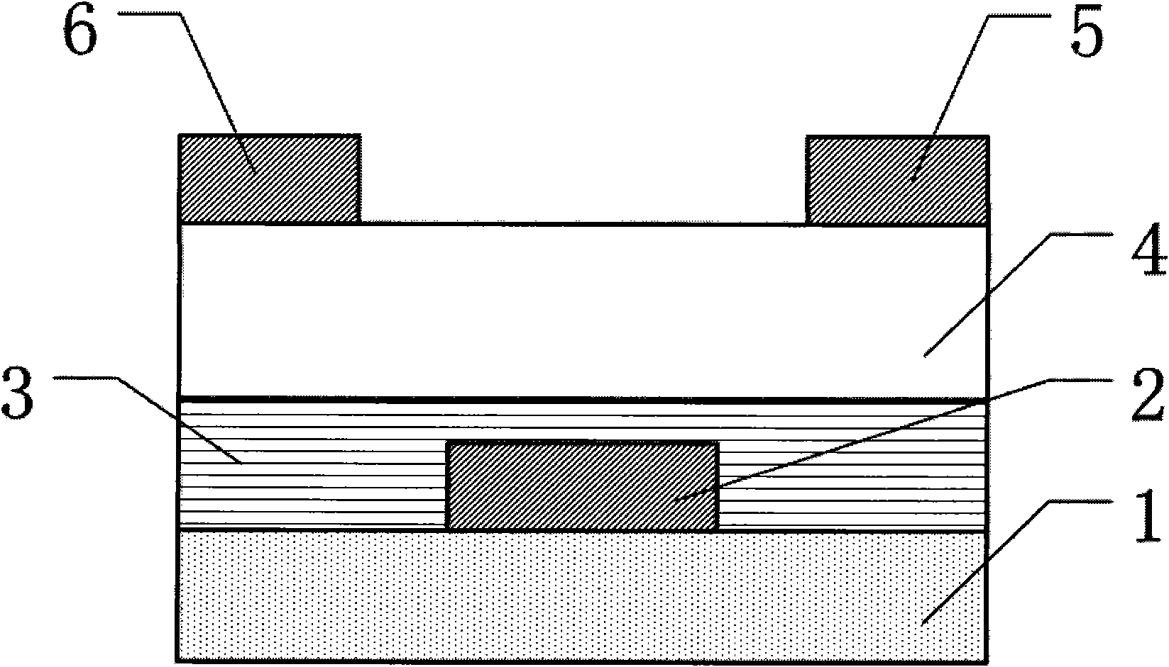
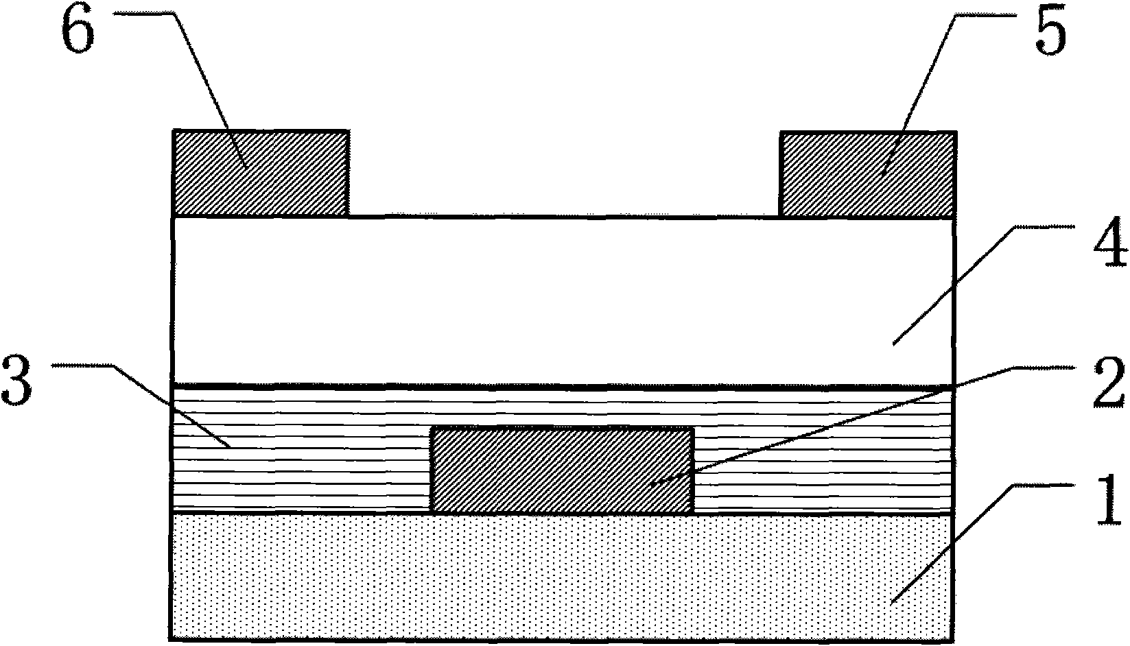
[0032] What is obtained by this preparation method is a bottom-contact quantum dot field effect transistor chiral sensor:
[0033] Step 1, sputtering or evaporating a layer of gate electrode 2 with a thickness of 10nm-500nm on the substrate 1, the gate electrode is composed of one or two of Ta, Ti, Cr, W, Mo, Au or Ag.
[0034] Step 2, sputtering or evaporating a layer of high dielectric constant gate insulating layer 3 with a thickness of 150nm to 500nm, the gate insulating layer is made of SiO 2 、 Ta 2 o 5 、Al 2 o 3 、TiO 2 , BZT, or PZT in one or two forms.
[0035] Step 3, sputtering, inkjet printing or evaporating a layer of source electrode 5 and drain electrode 6 composed of one or two of Au, Ag, Ti, PEDOT:PSS, etc. on the gate insulating layer 3 .
[0036] Step 4, on the gate insulating layer 3 and the source / drain electrodes, a layer of active layer 4 with a thickness of 10 nm to 500 nm is printed by vacuum thermal evaporation, spin coating, inkjet printing or scre...
PUM
Property
Measurement
Unit
Size
aaaaa
aaaaa
Abstract
The invention discloses a field effecttransistor chiral sensor and a manufacture method thereof. By utilizing the structure of a field effecttransistor, the chiral sensor comprises a substrate, a gate electrode, a gate insulating layer, an active layer, a source electrode and a drain electrode. The chiral sensor is characterized in that the active layer is made of a quantum dot material with chiral recognizing and detecting function. The quantum dot material of the active layer is a semiconductor nano microcrystal which is modified by chiral molecules and has the size of smaller than 100nm.The invention sensor capable of detecting a chiral substance by using a quantum dot film with the chiral recognizing and detecting function as the active layer of the field effecttransistor on the basis of the quantum dotfield effect transistor and the manufacture method thereof. The fluorescent chiral molecule modified quantum dot can be also made into a film by the chiral sensor for being used as the field effect transistor active layer, thereby overcoming the defect of chiral molecule detection by the traditional homogeneous phase fluorescent sensor and realizing a more stable detecting signal.
Description
technical field [0001] The invention relates to a sensor for chiral recognition research, in particular to a field effect transistor chiral sensor based on field effect transistor structure and application of quantum dot characteristics and a preparation method thereof. Background technique [0002] The unique properties of quantum dots are based on their own quantum effects. When the particle size enters the nanoscale, size confinement will cause size effects, quantum confinement effects, macroscopic quantum tunneling effects, and surface effects, thus deriving nanosystems with conventional The different low-dimensional physical properties of the system and the micro system show many physical and chemical properties different from those of the macroscopic material. It has extremely broad application prospects in nonlinear optics, magnetic media, catalysis, medicine and functional materials. The continuous development of science and information technology and basic research ...
Claims
Application Information
Patent Timeline
Application Date:The date an application was filed.
Publication Date:The date a patent or application was officially published.
First Publication Date:The earliest publication date of a patent with the same application number.
Issue Date:Publication date of the patent grant document.
PCT Entry Date:The Entry date of PCT National Phase.
Estimated Expiry Date:The statutory expiry date of a patent right according to the Patent Law, and it is the longest term of protection that the patent right can achieve without the termination of the patent right due to other reasons(Term extension factor has been taken into account ).
Invalid Date:Actual expiry date is based on effective date or publication date of legal transaction data of invalid patent.
IPC IPC(8): G01N27/414H01L29/78H01L21/336
Inventor潘革波王亦崔铮
OwnerSUZHOU INST OF NANO TECH & NANO BIONICS CHINESE ACEDEMY OF SCI

