Extensible oversize light-emitting diode (LED) chip and manufacture method thereof

A light-emitting diode, super-sized technology, used in semiconductor/solid-state device manufacturing, electrical components, electrical solid-state devices, etc. Effect

Active Publication Date: 2010-12-22
刘胜
View PDF8 Cites 29 Cited by
  • Summary
  • Abstract
  • Description
  • Claims
  • Application Information

AI Technical Summary

Problems solved by technology

It not only solves the problem of low light extraction efficiency when the chip size increases, but also ensures that good

Method used


Image

  • Extensible oversize light-emitting diode (LED) chip and manufacture method thereof
  • Extensible oversize light-emitting diode (LED) chip and manufacture method thereof
  • Extensible oversize light-emitting diode (LED) chip and manufacture method thereof

Examples


Embodiment 1

[0024] Embodiments of the present invention are further described below in conjunction with the accompanying drawings:

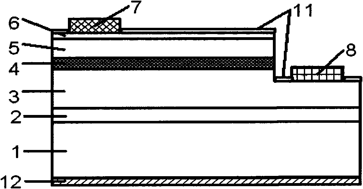
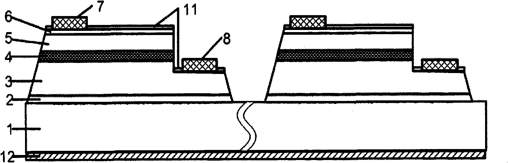
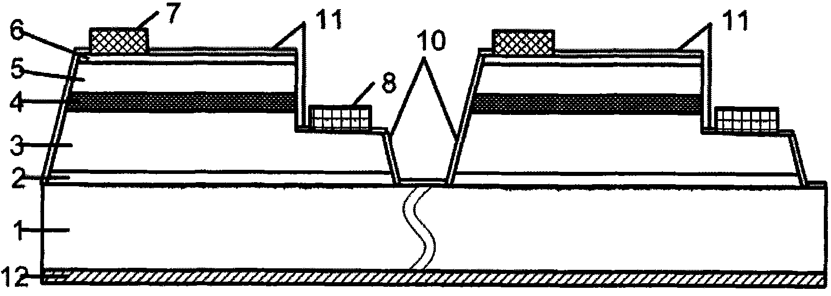
[0025] see figure 1 , figure 2 and image 3 It is a cross-sectional view of an expandable super-large-size light-emitting diode structure of the formal structure of the embodiment, Figure 4 , is the plan view of the expandable super-large-sized light-emitting diode of the formal structure of the embodiment. The shape of the chip is square, and the lateral dimension is 0.3 mm to 500 mm. This embodiment consists of a substrate 1, an epitaxially grown GaN buffer layer 2, an N-type doped GaN layer 3, an active layer 4, a P-type doped GaN layer 5, a current spreading layer 6, and a metal P electrode. 7, a metal N electrode 8, a protective film 11, and a reflective layer 12, and epitaxially grow a GaN buffer layer 2 on a sapphire substrate 1, an N-type doped GaN layer 3, an active layer 4, and a P Type doped gallium nitride layer 5, and then deposit a layer...

Embodiment 2

[0034] Embodiment 2 is the same as Embodiment 1, except that the shape of the chip is parallelogram or circle, and the shape of the groove 9 is comb-like, zig-zag or arc-like, see Figure 5 , Figure 6 , Figure 7 , the cross-section of the trench 9 is a positive trapezoid, and its inclination angle θ is 10° to 80°, and a reflective layer 12 is deposited on the side wall, see Figure 9 .


PUM

PropertyMeasurementUnit
Horizontal sizeaaaaaaaaaa

Abstract

The invention relates to an extensible oversize light-emitting diode (LED) chip which is characterized in that a buffer layer, an N-type doping layer, an active layer, a P-type doping layer and a current expanding layer which are laminated are formed on a substrate by epitaxial growth; a metal P electrode and a metal N electrode are formed by etching and depositing; a groove is formed between the P electrode and the N electrode by etching the chip; a reflecting layer is deposited on the side wall of the groove; and the reflecting layer is plated on the back of the substrate. The invention has the advantages that the groove etched on the chip can block the transverse transmission of light in the chip, the light extracting efficiency is improved, favorable current injection can be obtained, the chip is expanded to an oversize, and the manufacture process is simple.

Description

technical field [0001] The patent of the present invention relates to a semiconductor device and a manufacturing method, in particular to an expandable super-large-sized light-emitting diode chip and a manufacturing method. Background technique [0002] In recent years, semiconductor lighting has gradually been put on the agenda, and many countries and regions have started a certain range of applications and promotions. GaN-based light-emitting diodes and phosphors are mixed to produce white light technology, which has become the mainstream trend of current semiconductor lighting. . Gallium nitride-based light-emitting diodes have made great progress in all aspects in the past few years. The luminous efficiency of 1W high-power LEDs has been continuously improved. The lumen efficiency of commercial 1W high-power LED modules has exceeded 100lm / W, and the best level in the laboratory has even exceeded 140lm / W, which makes high-power nitrogen It is possible for GaN-based ligh...

Claims


Application Information

Patent Timeline
IPC IPC(8): H01L27/15H01L33/00H01L21/8252H01L21/306
Inventor 刘胜魏巍王恺汪沛周圣军曹斌甘志银
Owner 刘胜
Why Eureka
Try Eureka