Gas input device and plasma processing equipment

An input device and gas technology, applied in the direction of electrical components, discharge tubes, circuits, etc., can solve the problems of differences in the rate and uniformity of etching or deposition on the wafer surface, affecting the processing quality of semiconductor wafers, and uneven gas flow distribution. Achieve the effects of avoiding uneven gas distribution, uniform process gas pressure and flow distribution, and similar etching or deposition rates

Inactive Publication Date: 2010-12-29
BEIJING NAURA MICROELECTRONICS EQUIP CO LTD
View PDF0 Cites 10 Cited by
  • Summary
  • Abstract
  • Description
  • Claims
  • Application Information

AI Technical Summary

Problems solved by technology

[0005] The above-mentioned inductively coupled plasma device adopts the method of air intake in the upper center of the reaction chamber 3. Although the nozzle 2 can be provided with multiple air inlets, the problem is that the nozzle 2 is fixedly installed in the center of the quartz cover plate, and the process gas enters the reaction chamber. After the chamber 3, the difference in the length of the gas flow path from the center of the wafer 7 to the edge will cause the gas flow field on the surface of the wafer 7 to form a gradient distribution from the center to the edge, so that the concentration of the process gas is higher at the center of the wafer 7 and lower at the edge , the air flow distribution above the surface of the entire wafer 7 is uneven, which affects the processing quality of the semiconductor wafer 3
[0006] Since the plasma participating in the reaction is formed by the ionization of the process gas, the above-mentioned non-uniform gas flow distribution will lead to great differences in the rate and uniformity of etching or deposition on the entire wafer surface, thus affecting the quality of wafer processing Rate

Method used


Image

  • Gas input device and plasma processing equipment
  • Gas input device and plasma processing equipment
  • Gas input device and plasma processing equipment

Examples


Embodiment Construction

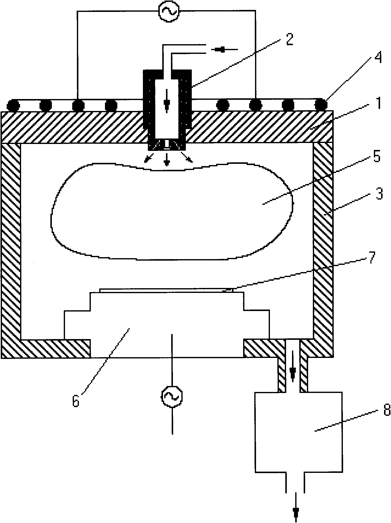
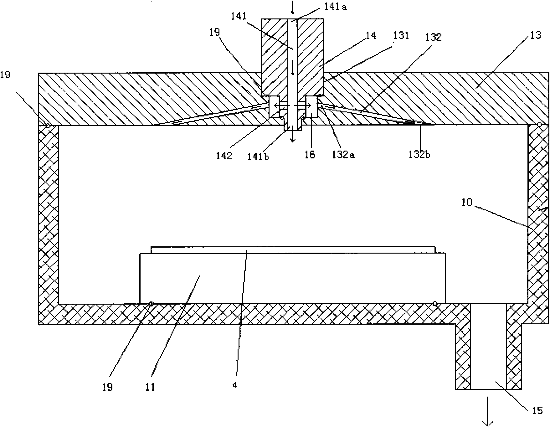
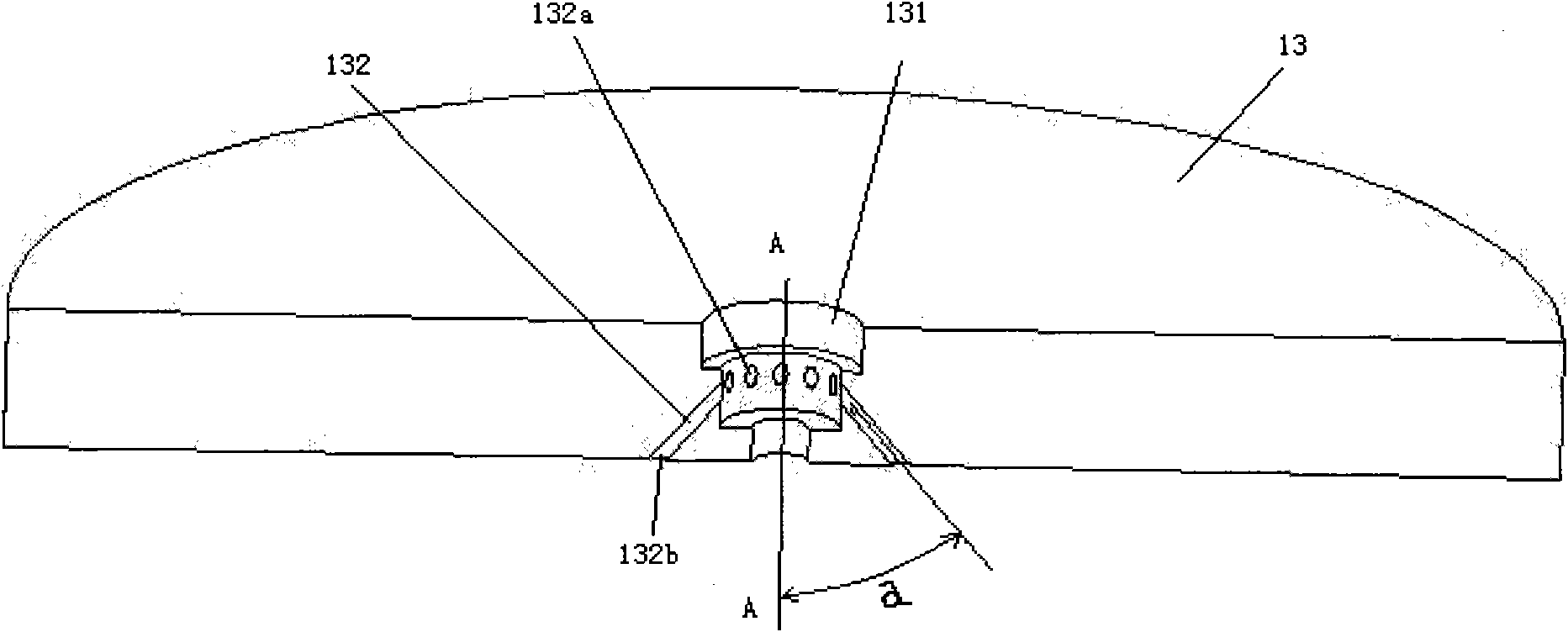
[0033] In order to make the above objects, features and advantages of the present invention more comprehensible, specific implementations of the present invention will be described in detail below in conjunction with the accompanying drawings.

[0034] In the following description, many specific details are set forth in order to fully understand the present invention, but the present invention can also be implemented in other ways than those described here, so the present invention is not limited by the specific embodiments disclosed below.

[0035] Secondly, the present invention is described in detail in conjunction with schematic diagrams. When describing the embodiments of the present invention in detail, for the convenience of explanation, the sectional view showing the structure of the device will not be partially enlarged according to the general scale, and the schematic diagram is only an example, and it should not be limited here. The protection scope of the present in...


PUM


Abstract

The invention provides a gas input device and plasma processing equipment. The gas input device comprises a nozzle and a cover plate, wherein, the nozzle is provided with a first channel and a nozzle bypass communicated with the first channel; the cover plate is provided with a groove and a plurality of second channels, the groove is basically arranged at the central position of the cover plate, and the plurality of the second channels are uniformly distributed in the cover plate around the center line of the groove; and the nozzle is embedded into the groove, the air outlet end of the first channel stretches out of the cover plate from the bottom part of the groove, and the air inlet ends of the plurality of the second channels are communicated with the nozzle bypass. The gas input device and the plasma processing equipment can obtain uniform air flow distribution above the whole surface of a processed wafer so as to effectively avoid non-uniform etching or deposition caused by non-uniform gas distribution from the center to the edge above the wafer surface, thus promoting the etching or deposition rate of points on the whole wafer surface to be more similar.

Description

technical field [0001] The invention relates to the technical field of plasma processing, in particular to a gas input device and plasma processing equipment. Background technique [0002] In the manufacturing process of integrated circuits and solar cells, it is usually necessary to use plasma processing equipment to perform thin film deposition, etching and other processing processes on semiconductor wafers such as single crystal silicon. In the plasma processing equipment, the gas input device usually provides the required process gas for the processing of the semiconductor wafer, and can also provide the required auxiliary gas under certain circumstances or during equipment maintenance. [0003] Currently, plasma processing equipment is widely used in the manufacturing process of integrated circuits or MEMS devices. For example, inductively coupled plasma devices are usually used in dry etching (Dry Etching) or chemical vapor deposition (CVD) processes. The principle is...

Claims


Application Information

Patent Timeline
Patent Type & Authority Applications(China)
IPC IPC(8): H01J37/02H01J37/32
Inventor 林挺昌
Owner BEIJING NAURA MICROELECTRONICS EQUIP CO LTD
Why Eureka
Try Eureka