Single-sided chemically mechanical polishing method and device of silicon chip

A technology of chemical machinery and polishing equipment, which is applied in the direction of grinding equipment, grinding machine tools, metal processing equipment, etc., can solve the problems of low cleaning quality of silicon wafers in the post-cleaning system, affecting the surface quality of silicon wafers, and increasing the residence time of silicon wafers. Achieve single-side polishing quality and stability, improve single-side polishing quality, and achieve high-quality single-side polishing

Inactive Publication Date: 2011-01-05
THE 45TH RES INST OF CETC
View PDF7 Cites 20 Cited by
  • Summary
  • Abstract
  • Description
  • Claims
  • Application Information

AI Technical Summary

Problems solved by technology

The disadvantage of this polishing process is: the residence time of the silicon wafer in the secondary polishing process increases, and after the initial polishing, the residual polishing liquid on the silicon wafer will further corrode the silicon wafer

Method used


Image

  • Single-sided chemically mechanical polishing method and device of silicon chip
  • Single-sided chemically mechanical polishing method and device of silicon chip
  • Single-sided chemically mechanical polishing method and device of silicon chip

Examples


Embodiment 1

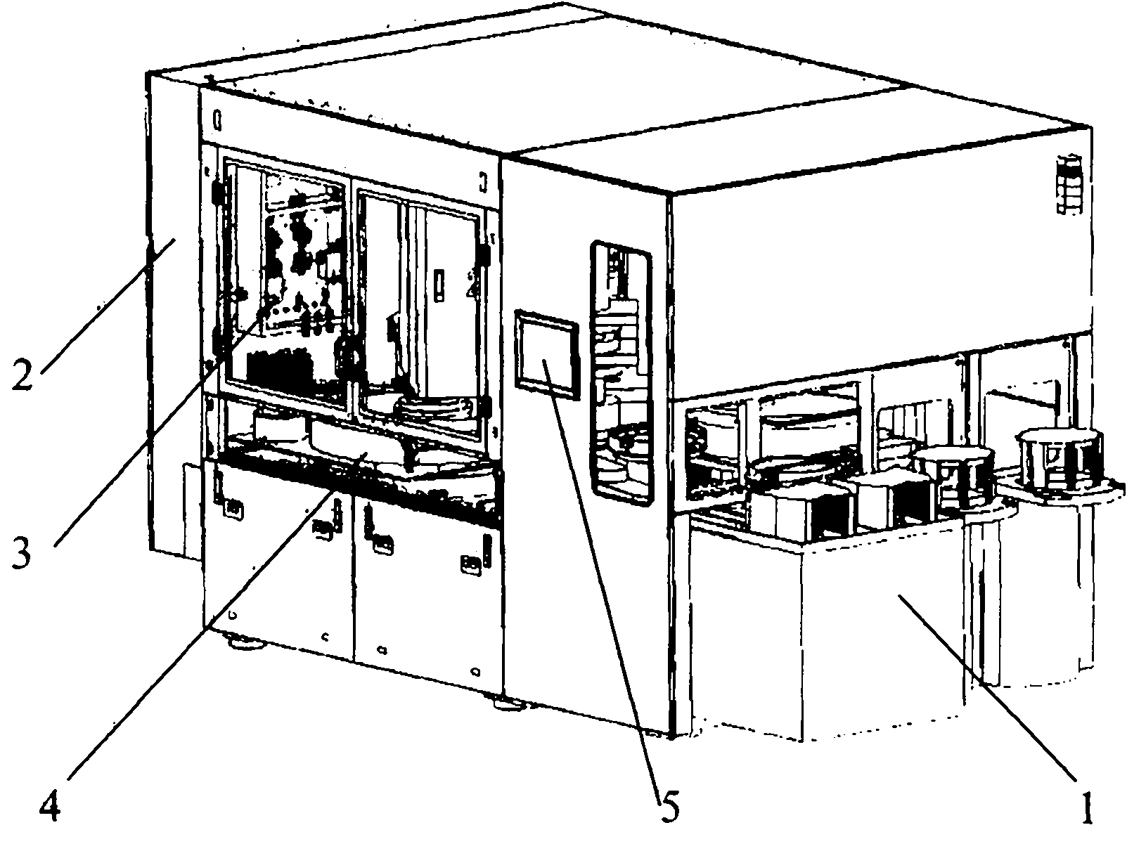
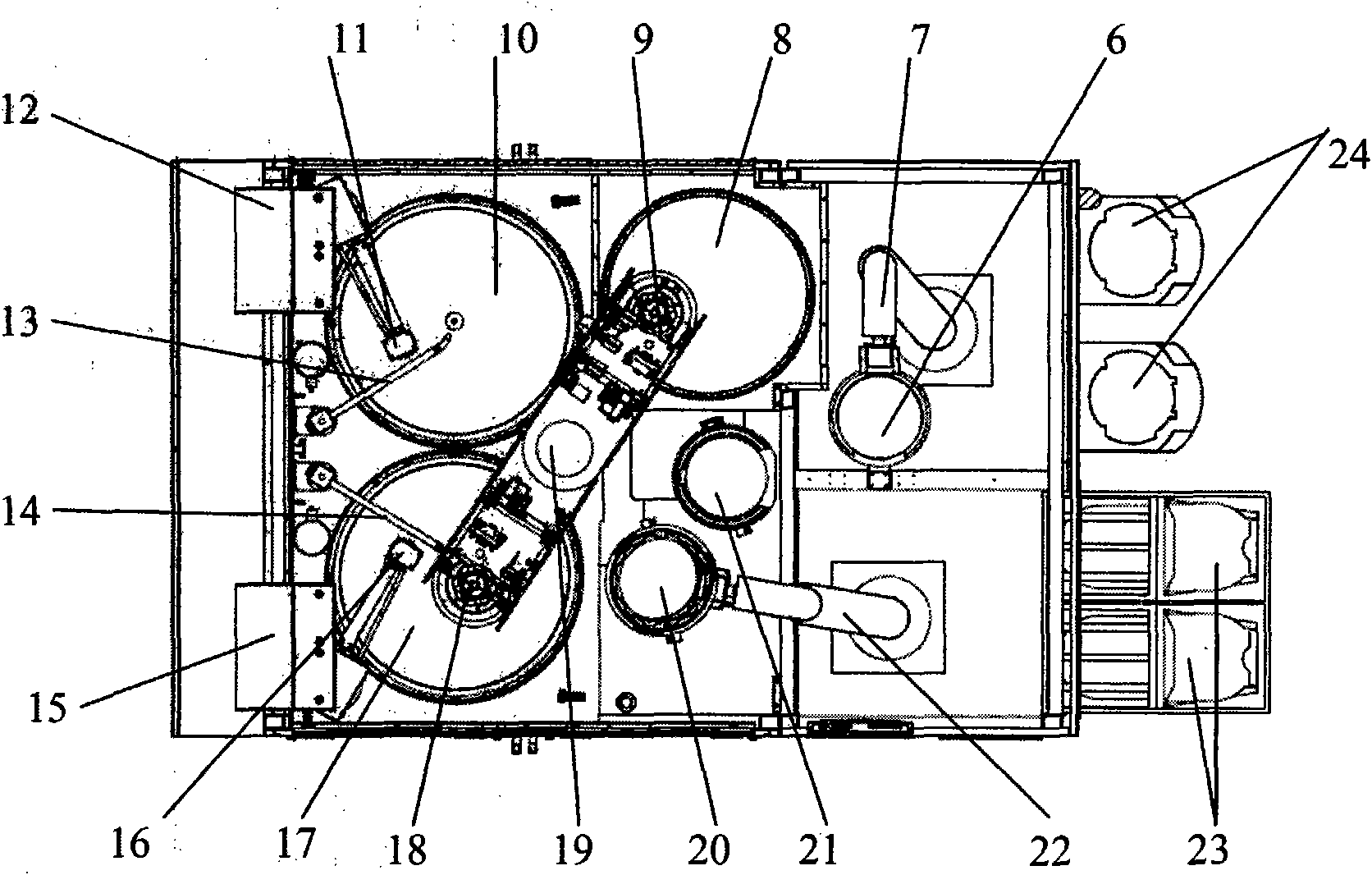
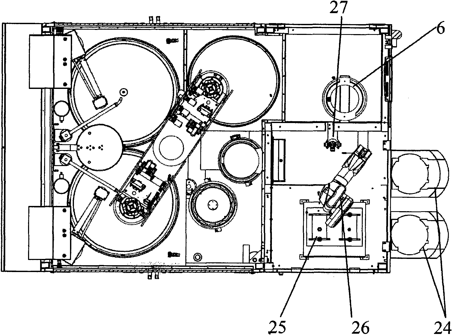
[0037] The silicon wafer single-side chemical mechanical polishing device mainly includes a preliminary polishing table 17 and / or a finishing polishing table 10 , a polishing liquid supply mechanism, an electrical control part, and a rinsing and polishing table 8 . The rinse-polish table 8 has a deionized water rinse-polish supply mechanism. The primary polishing table and the finishing polishing table are independently provided with 2 or more than 3 polishing liquid supply mechanisms, and have a structure for supplying polishing liquid by combining them. The polishing heads on the preliminary polishing table 17, the fine polishing table 10 or the rinsing polishing table 8 are all connected with the polishing spindle rotation, lifting and air suction mechanism, and the polishing spindle rotation, lifting and air suction mechanism are all installed in the rotatable turret 19 above; the silicon wafer reprinting part is equipped with a silicon wafer loading station (LoadStation),...

Embodiment 2、 Embodiment 3

[0070] Embodiment 2 and Embodiment 3: the combination of the preliminary polishing table 17 and the rinsing and polishing table 8, and the combination of the finishing polishing table 10 and the rinsing and polishing table 8.

[0071] The process flow of single polishing and rinsing and polishing combined method adopted by this system equipment is basically similar to that of double polishing and rinsing and polishing combined method. After the silicon wafer is polished once on the primary polishing table 17 or the finishing polishing table 10, the polishing head carrier B18 is directly rotated to the rinsing table 8 for rinsing and polishing. In the process flow of single polishing and rinsing and polishing combination method, the descriptive name of preliminary polishing station 17 or finishing polishing station 10 does not mean that the initial polishing or finishing polishing process will be completed, but only in the description of the double polishing and rinsing and poli...


PUM


Abstract

The invention provides single-sided chemically mechanical polishing method and device of a silicon chip, belonging to the technical field of single-sided chemically mechanical polishing methods and apparatuses of the silicon chip. The method comprises the following steps of: carrying out primary polishing and/or fine polishing according to surface quality requirements of single-sided polishing of the silicon chip and then carrying out rinsing polishing on a silicon chip. The device mainly comprises a primary polishing table and/or a fine polishing table and a rinsing polishing table. The invention can effectively reduce or eliminate residues of a polishing solution on a silicon chip surface after the silicon chip is primarily polished or finely polished, can greatly improve the single-sided polishing quality of the silicon chip, has wide application and can particularly satisfy higher precision requirements of the silicon chip with a diameter of 300 mm and above on overall and partial flatness and micro-roughness, and the like; the method is reasonable, unique in principle and favorable in processibility; the device has simple structure, reasonable configuration and high and stable single-sided polishing quality and is beneficial to enhancing production efficiency, reducing costs and realizing automation in the production process.

Description

technical field [0001] The invention belongs to the technical field of chemical mechanical polishing methods and equipment for silicon wafers, in particular to a method and device for chemical mechanical polishing of silicon wafers. Background technique [0002] The traditional production process of silicon wafers is usually mainly completed by single crystal growth, slicing, chamfering, polishing, cleaning and final packaging, and each process is supported by corresponding equipment. [0003] With the rapid development of integrated circuit manufacturing technology and the increase of the diameter of silicon wafers, higher requirements are placed on the surface quality of silicon wafers. The 200mm silicon wafer can meet the application requirements through the double-sided grinding and polishing process of the silicon wafer. But for 300mm silicon wafers, the front side of the silicon wafer not only requires high global flatness accuracy, but also requires higher local flat...

Claims


Application Information

Patent Timeline
IPC IPC(8): B24B37/04
CPCB24B37/10
Inventor 柳滨李伟郭强生廖垂鑫
Owner THE 45TH RES INST OF CETC
Why Eureka
Try Eureka