Shift register circuit, display device, and method for driving shift register circuit

A shift register, driving method technology, applied in static memory, digital memory information, instruments, etc., can solve problems such as loss of switching function, difficult node netA connection, malfunction, etc., to achieve good display, improve circuit characteristics, and operate stably Effect

Inactive Publication Date: 2011-01-05
SHARP KK
View PDF3 Cites 21 Cited by
  • Summary
  • Abstract
  • Description
  • Claims
  • Application Information

AI Technical Summary

Problems solved by technology

When the transistor that connects the output terminal Gn to the low level has a threshold voltage shift phenomenon, it gradually becomes difficult to transition to the on state, and it becomes difficult to connect the output terminal Gn to the low level.
In addition, when the threshold voltage shift phenomenon occurs in the transistor that connects the node netA to the low level, it gradually becomes difficult to transition to the on state, and it becomes difficult to connect the node netA to the low level. Therefore, if the node If the potential of netA rises due to potential instability or leakage of each transistor, etc., the output transistor ( Figure 7 The transistor Tr4 in the middle) will leak, so it is still difficult to keep the output terminal Gn at a low level
[0016] Due to this threshold voltage shift phenomenon, the TFT that has been applying a DC bias voltage to the gate will lose its switching function during long-term operation, and eventually the shift register circuit cannot perform its original function and cause malfunction.
As a result, it is impossible to suppress the occurrence of crosstalk on the gate bus line due to potential fluctuations in the source bus line, etc., and stable display cannot be performed.

Method used


Image

  • Shift register circuit, display device, and method for driving shift register circuit
  • Shift register circuit, display device, and method for driving shift register circuit
  • Shift register circuit, display device, and method for driving shift register circuit

Examples


Embodiment Construction

[0099] Below, based on Figure 1 to Figure 5 , an embodiment of the present invention is described.

[0100] Figure 5 The structure of the liquid crystal display device 11 which is the display device of this embodiment is shown in FIG.

[0101] The liquid crystal display device 11 includes a display panel 12 , a flexible printed substrate 13 , and a control substrate 14 .

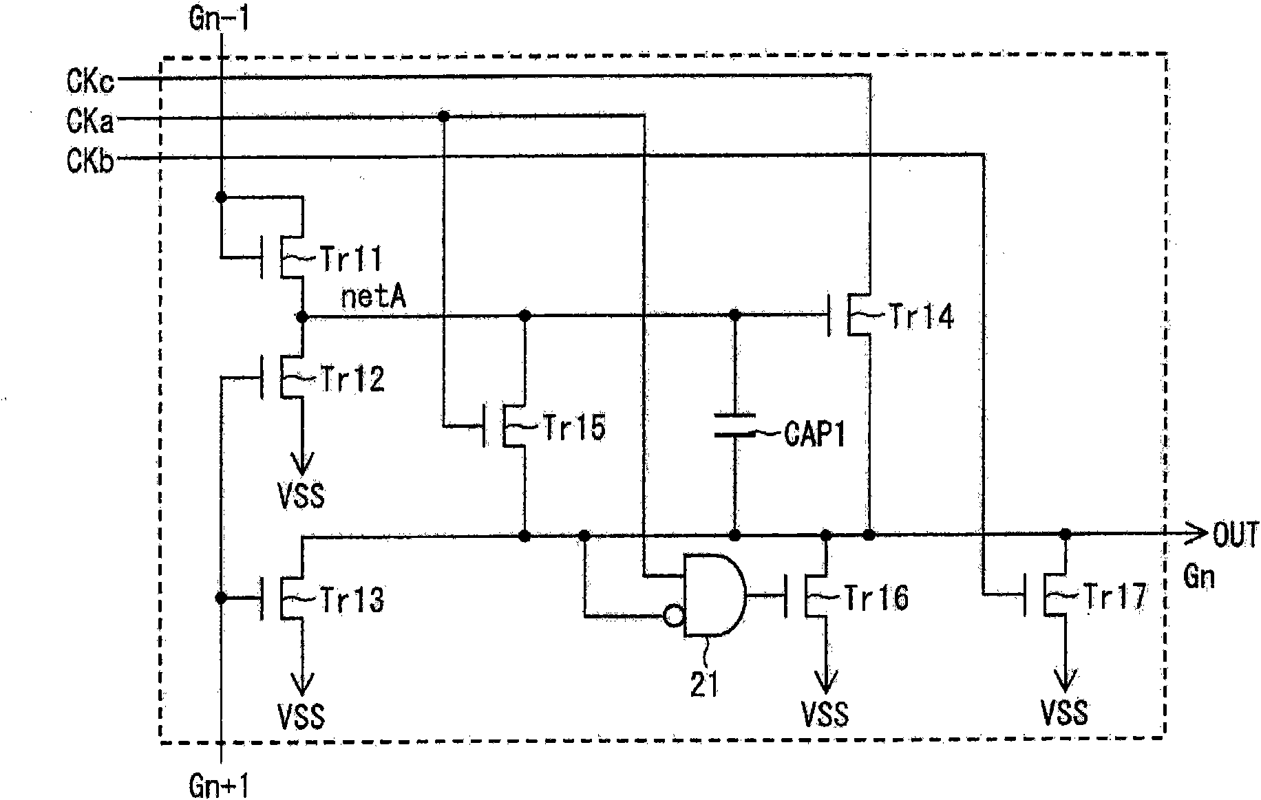
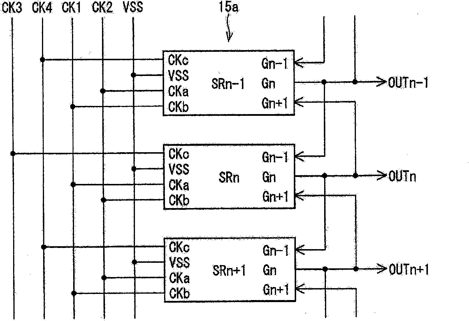
[0102] The display panel 12 is formed on a glass substrate using amorphous silicon, polysilicon, CG silicon, microcrystalline silicon, etc. to form a display area 12a, a plurality of gate lines (scanning signal lines) GL..., and a plurality of source lines (data signal lines). )SL . . . and an active matrix display panel of a gate driver (scanning signal line driver circuit) 15 . The display area 12a is an area in which a plurality of pixels PIX are arranged in a matrix. The pixel PIX includes a TFT 21 as a pixel selection element, a liquid crystal capacitor CL, and an auxiliary capacitor Cs. The gate...


PUM


Abstract

The invention discloses a shift register circuit, a display device, and a method for driving the shift register circuit. In at least one embodiment, each of stages connected in cascade includes a first circuit which causes a predetermined section in a corresponding one of the stages to be connected to a low-potential power source, the first circuit being constituted by TFTs, a first type of clock signal being used as a signal which is transferred to an output terminal of each of the stages so as to be outputted as an output signal, a second type of clock signal being used as a signal which drives the first circuit. With the arrangement, it is possible to realize a shift register circuit that is capable of further suppressing a shift phenomenon of a threshold voltage in each of the TFTs.

Description

technical field [0001] The present invention relates to a shift register circuit fabricated as a single piece in a display panel. Background technique [0002] In recent years, the gate driver is formed on a liquid crystal panel using amorphous silicon to achieve cost reduction. Gate monolithic is also called gate driverless, gate driver built in panel, gate in panel, etc. [0003] Image 6 A configuration example of a shift register circuit constituting a gate driver formed of a single piece of gate is shown in FIG. [0004] In this shift register circuit, each stage of SR (..., SRn-1, SRn, SRn+1,...) has a set input terminal Gn-1, an output terminal Gn, a reset input terminal Gn+1, and a low power Flat power input terminal VSS and clock signal input terminal CK. The output signal OUT (..., OUTn-1, OUTn, OUTn+1,...) of the previous stage is input to the set input terminal Gn-1. The output terminal Gn outputs the output signal OUT to the corresponding scanning signal lin...

Claims


Application Information

Patent Timeline
Patent Type & Authority Applications(China)
IPC IPC(8): G11C19/28G09G3/20G09G3/36G11C19/00
CPCG11C19/28G09G2300/0408G09G2310/0286G09G2300/0417G09G2310/08G09G3/3677
Inventor 森井秀树岩本明久水永隆行太田裕己广兼正浩田中信也今井元菊池哲郎
Owner SHARP KK
Why Eureka
Try Eureka