Preparation method of high-uniformity copper-indium-gallium-selenium (CIGS) absorbed layer

A technology of copper indium gallium selenide and absorbing layer, which is applied in the field of solar power generation, and can solve problems such as huge equipment, low utilization rate of sputtering targets, and long CIGS thin film time

Inactive Publication Date: 2011-01-12
ZHEJIANG SHANGYUE OPTOELECTRONICS TECH
View PDF1 Cites 13 Cited by
  • Summary
  • Abstract
  • Description
  • Claims
  • Application Information

AI Technical Summary

Problems solved by technology

The disadvantage of this technology is that the equipment is relatively large, the equipment investment is large, the prepa

Method used


Image

  • Preparation method of high-uniformity copper-indium-gallium-selenium (CIGS) absorbed layer
  • Preparation method of high-uniformity copper-indium-gallium-selenium (CIGS) absorbed layer

Examples


Embodiment Construction

[0021] The present invention will be further described below in conjunction with the accompanying drawings and embodiments, but not as a basis for limiting the present invention.

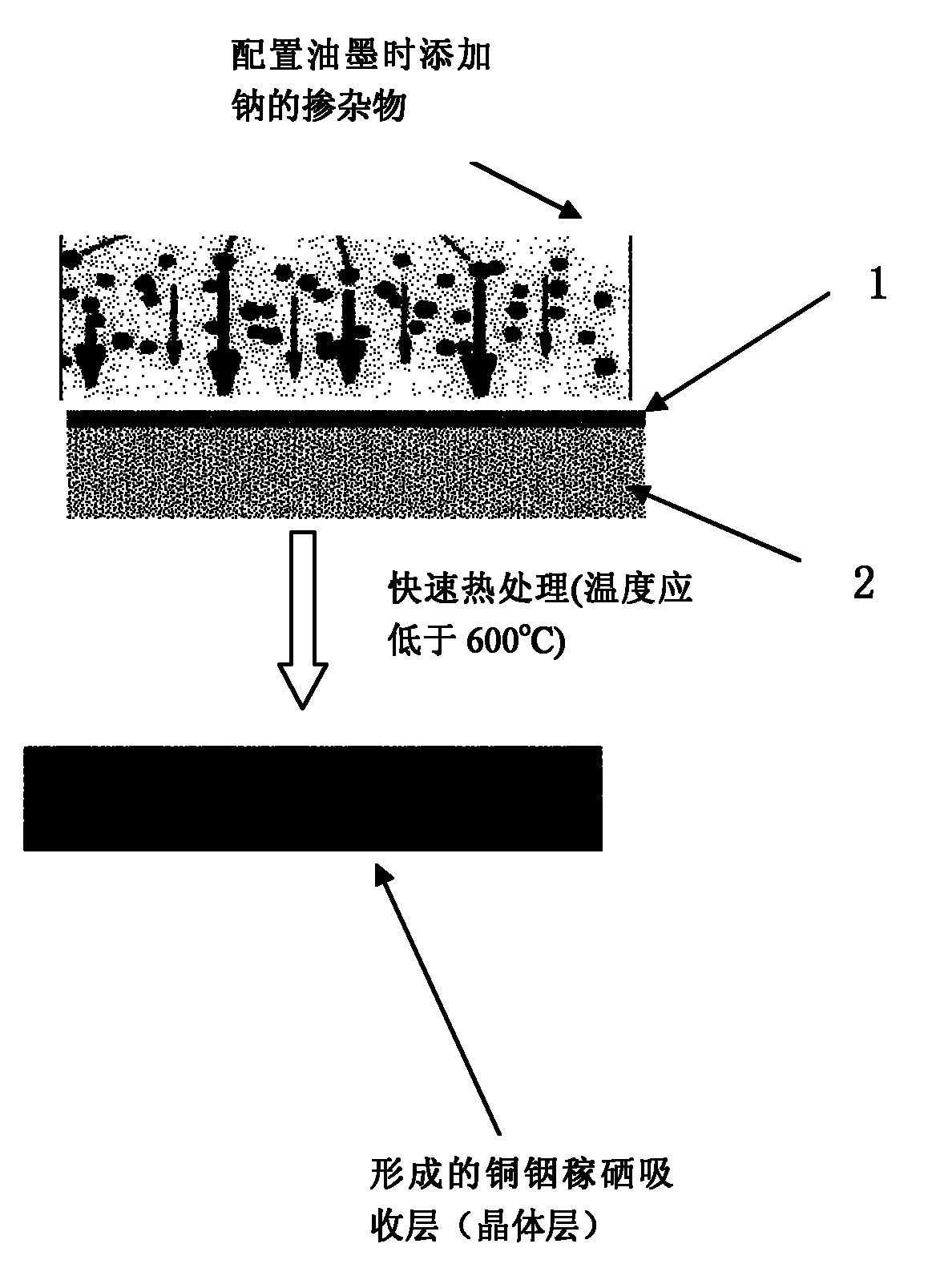
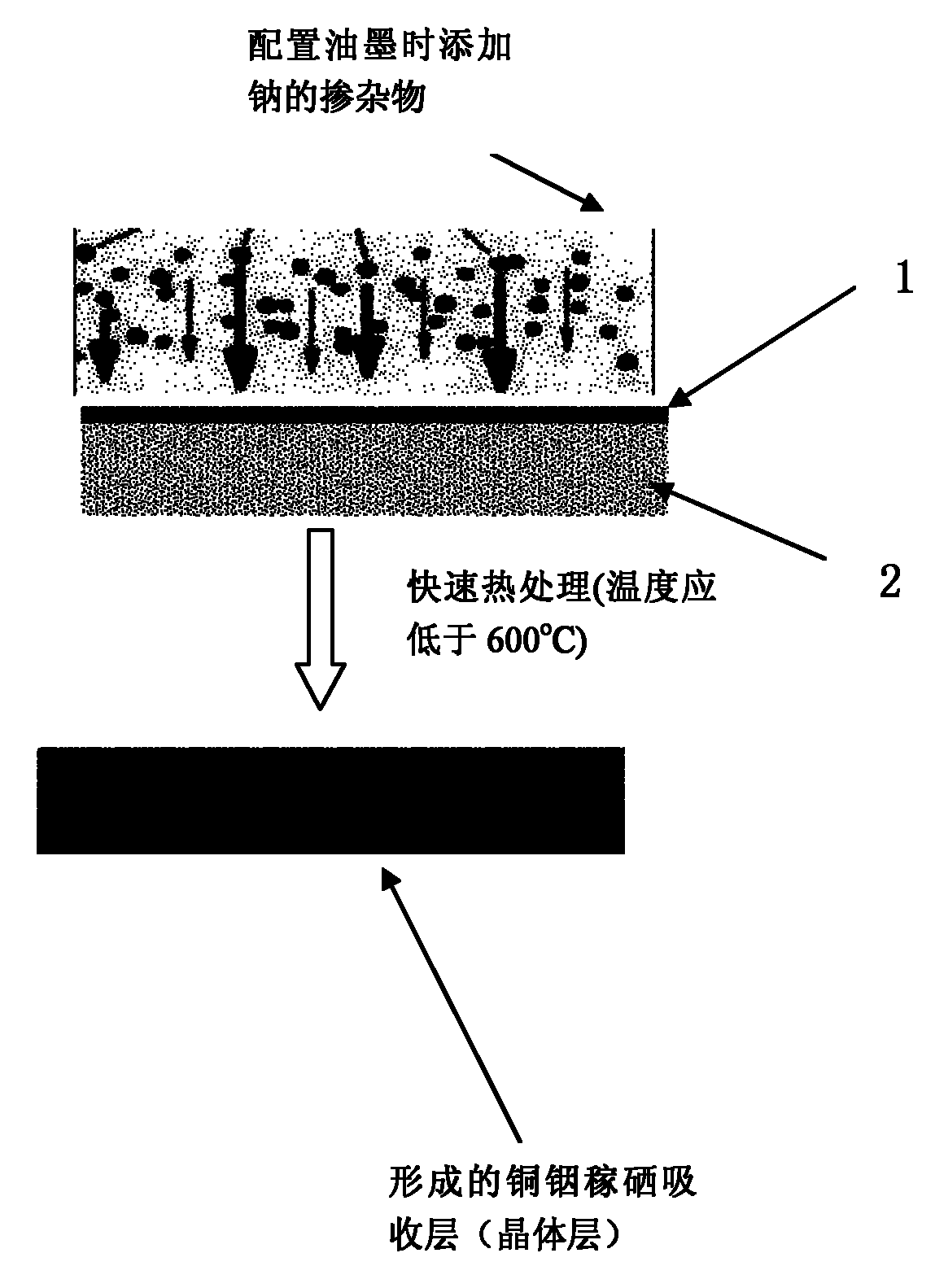
[0022] Example. A method for preparing a high-uniformity copper indium gallium selenide absorbing layer, such as figure 1 As shown, the method includes the following steps:

[0023] A. Use copper, indium, gallium and selenium nanoparticles, or copper, indium, gallium and selenium binary, ternary or quaternary alloy nanoparticles to make ink X, ink X contains copper, indium, gallium and selenium Four elements; use selenium nanoparticles to make ink Y; sodium dopant added when configuring ink X layer;

[0024] B. Spray the ink X and ink Y prepared in step A on the flexible metal film by using a simple multi-layer printing method;

[0025] C. Rapid heat treatment, melting and mixing of nanoparticles in ink X and ink Y;

[0026] D. Annealing to form a uniform copper indium gallium selenide absorptio...


PUM


Abstract

The invention discloses a preparation method of a high-uniformity copper-indium-gallium-selenium (CIGS) absorbed layer, which is characterized by comprising the following steps: preparing printing ink by using CIGS containing different particle sizes or binary, ternary and quaternary alloy nanoparticles thereof, preparing the CIGS absorbed layer of a thin film solar cell by using a simple multilayer jet-printing method, and enhancing the grain structure and film forming uniformity of the CIGS absorbed layer through rapid heat treatment. In the invention, the CIGS absorbed layer is prepared under a non-vacuum condition, thus avoiding using expensive vacuum equipment; and the preparation method has the advantages of simple process and easy control and can help obtain the high-uniformity CIGS absorbed layer.

Description

technical field [0001] The invention relates to a method for preparing a high-uniformity copper indium gallium selenium absorbing layer, which belongs to the technical field of solar power generation. Background technique [0002] Copper indium gallium selenium thin film solar cells have the characteristics of low production cost, less pollution, no fading, and good weak light performance. It is called "a very promising new thin-film solar cell in the next era" internationally. In addition, the battery has a soft and uniform black appearance, which is an ideal choice for places with high requirements on appearance, such as glass curtain walls of large buildings, etc., and has a large market in modern high-rise buildings and other fields. Copper indium gallium selenide thin film solar cells usually include a substrate, a bottom electrode layer (Mo), a light absorbing layer (CIGS), a buffer layer (ZnS or CdS), a transparent conductive film layer and an anti-reflective layer. ...

Claims


Application Information

Patent Timeline
IPC IPC(8): H01L31/18C22F1/00
CPCY02P70/50
Inventor 任宇航任宇珂
Owner ZHEJIANG SHANGYUE OPTOELECTRONICS TECH
Why Eureka
Try Eureka