
Bootstrap switch circuit

A bootstrap switch, circuit technology, applied in the direction of conversion equipment without intermediate conversion to AC, can solve problems such as affecting circuit reliability and increasing power consumption

Active Publication Date: 2013-03-20
3PEAK INC
View PDF0 Cites 0 Cited by
  • Summary
  • Abstract
  • Description
  • Claims
  • Application Information

AI Technical Summary

Problems solved by technology

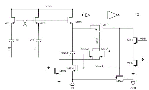
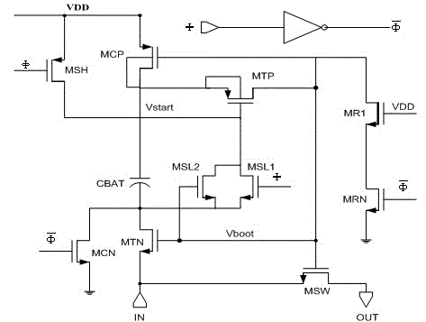
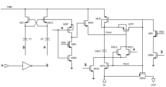
But the transistor MSH in its start-up circuit is a PMOS transistor. When the signal level exceeds the power supply level, the Vstart level will be close to twice the power supply voltage VDD, which will turn on the parasitic diode from the drain of the transistor MSH to the N well, so that The gate voltage of the main switching transistor MSW is limited, increasing power consumption and affecting the reliability of the circuit

Method used


Image

  • Bootstrap switch circuit
  • Bootstrap switch circuit
  • Bootstrap switch circuit

Examples


Embodiment Construction

[0027] From the purpose of the present invention, a bootstrap switch circuit is proposed, which can use smaller chip area and power consumption to support the chip with a higher input signal range and maintain a faster response speed. The bootstrap switch circuit can extend the low-power SAR ADC range beyond the supply voltage, allowing it to have a larger dynamic range while minimizing power loss, which plays an important role in the power management of increasingly large-scale integrated circuits. In the prior art, many solutions have been designed one-sidedly to solve the problems of switch connection power supply and charging capacitor, etc., but the optimal design of chip size and power consumption has not been taken into account. Since there is no static power consumption and no influence from the parasitic body diode that is turned on when the input voltage is greater than the power supply voltage, the bootstrap switch circuit provided by the present invention has a desi...


PUM


Abstract

The invention discloses a bootstrap switch circuit, which comprises a bootstrap switch coupled between an input node and an output node, a first transistor coupled to the control node of the bootstrap switch, a first capacitor coupled to the first transistor, a second transistor coupled between the control node of the first transistor and a power supply node and provided with a control node coupled to a first clock signal node, a third transistor coupled between the control node of the first transistor and the power supply node, a starting circuit provided with a second end coupled to the control node of the first transistor, a charge pump and a level shifter provided with a second output coupled with the control node of the starting circuit. The bootstrap switch circuit generates double power supply voltage by using the charge pump to switch on the starting circuit so as to feasibly fulfill the purpose of supporting a larger input signal range with small chip area and keep higher response speed.

Description

technical field [0001] The invention relates to integrated electronic circuit design, in particular to a bootstrap switch circuit design with low power consumption and large signal input range. Background technique [0002] Highly integrated power management applications often require the ability to have a large signal input range of voltage quantities, which is fundamentally due to the ability to operate at the lowest possible supply voltage while still maintaining sampling and data measurement of the environment exceeding the supply voltage. An essential requirement for operating power management ICs to maximize efficiency. [0003] In today's highly integrated power management applications, low power successive approximation register (SAR) analog-to-digital converters (ADCs) are often used to monitor on-chip and off-chip voltage quantities. This requirement often extends the range of the upper ADC to sample inputs greater than the supply voltage. The ADC must run at the...

Claims


Application Information

Patent Timeline
Patent Type & Authority Patents(China)
IPC IPC(8): H02M3/07
Inventor 刘扬应峰何德军周之栩牟陟
Owner 3PEAK INC
Learn More