CMOS (Complementary Metal Oxide Semiconductor) device and manufacturing method thereof

A manufacturing method and device technology, applied in semiconductor/solid-state device manufacturing, electrical solid-state devices, semiconductor devices, etc., can solve problems such as affecting CMOS performance, serious bottom leakage current, etc., to improve mobility, improve response speed, and solve the problem of lining Effect of bottom leakage current problem

Inactive Publication Date: 2011-01-26
SEMICON MFG INT (SHANGHAI) CORP
View PDF0 Cites 11 Cited by
  • Summary
  • Abstract
  • Description
  • Claims
  • Application Information

AI Technical Summary

Problems solved by technology

However, this technology has the following problems: the bottom of the NMOS transistor is formed with a buried oxide layer 2, which can effectively eliminate the substrate leakage current, and because the PMOS transistor is directly formed on the surface of the underlying silicon 1, the bottom leakage current will be very serious, which will affect the CMOS. performance

Method used


Image

  • CMOS (Complementary Metal Oxide Semiconductor) device and manufacturing method thereof
  • CMOS (Complementary Metal Oxide Semiconductor) device and manufacturing method thereof
  • CMOS (Complementary Metal Oxide Semiconductor) device and manufacturing method thereof

Examples


Embodiment Construction

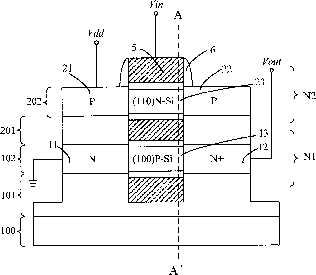
[0049] Existing composite substrate CMOS devices, because there is always a transistor directly formed on the silicon substrate, and the leakage current of the substrate is easy to occur, the CMOS device of the present invention stacks transistors on the silicon-on-insulator, and uses different The crystal orientation and layers of the top layer of silicon are used as the base of each transistor to form a conductive channel, supplemented by a multi-layer buried oxide layer to insulate the base, so as to solve the above-mentioned leakage current problem.

[0050] Such as image 3 Shown is the cross-sectional structure diagram of the CMOS device of the present invention, Figure 4 for along image 3 The cross-sectional schematic diagram of the A-A' section in the middle, combined with image 3 as well as Figure 4 , the CMOS device of the present invention specifically includes:

[0051] A silicon substrate 100, a first buried oxide layer 101, a first top layer silicon 102, ...


PUM

PropertyMeasurementUnit
thicknessaaaaaaaaaa
thicknessaaaaaaaaaa
sizeaaaaaaaaaa

Abstract

The invention relates to a CMOS (Complementary Metal Oxide Semiconductor) device and a manufacturing method thereof. The CMOS device comprises a silicon substrate, as well as a first buried oxide layer, first top layer silicon, a second buried oxide layer and second top layer silicon which are arranged on the silicon substrate in sequence, wherein the first top layer silicon and the second top layer silicon are different in 3.3 crystallographic orientation; a first field effect transistor is formed on the first top layer silicon used as a substrate, a second field effect transistor is formed on the second top layer silicon used as a substrate and is aligned to the first field effect transistor, and the conduction types of the first field effect transistor and the second field effect transistor are different. In the provided CMOS device, the crystallographic orientations of substrates of conducting channels formed by NMOS (N-Channel Metal Oxide Semiconductor) transistors and PMOS (P-Channel Metal Oxide Semiconductor) transistors are respectively (100) and (110), so that the mobility of respective current carrier is increased, and the response speed of the CMOS device is increased. The problem of current leakage of the substrates is solved by insulating the substrate of each transistor through stacking the transistors and using multiple buried oxide layers.

Description

technical field [0001] The invention relates to a semiconductor CMOS process, in particular to a CMOS device and a manufacturing method thereof. Background technique [0002] Complementary Metal Oxide Semiconductor (CMOS: Complementary Metal Oxide Semiconductor) devices are the basis of modern semiconductor integrated circuit technology and constitute the most basic unit of digital integrated circuits. CMOS devices are an organic combination of NMOS transistors and PMOS transistors to form logic devices. Its advantage is that only when the logic state transitions, a large current will be generated, and in a stable logic state, only a very small current will pass. Therefore, The power consumption of the logic circuit can be greatly reduced. [0003] Such as figure 1 As shown, the structure of a typical existing CMOS device (inverter) includes an NMOS transistor M1 and a PMOS transistor M2 connected in series, one end of which is grounded, and the other end is connected to a...

Claims


Application Information

Patent Timeline
Patent Type & Authority Applications(China)
IPC IPC(8): H01L27/12H01L29/04H01L29/06H01L21/84
Inventor 肖德元季明华吴汉明
Owner SEMICON MFG INT (SHANGHAI) CORP
Why Eureka
Try Eureka