

Automatic focusing method and device for lithography machine
A technology of automatic focusing and lithography, which is applied in opto-mechanical equipment, optics, instruments, etc., and can solve the problems of small measurement range, low measurement accuracy, and complex structure.
- Summary
- Abstract
- Description
- Claims
- Application Information
AI Technical Summary
Problems solved by technology
Method used
Image

Examples
Embodiment Construction
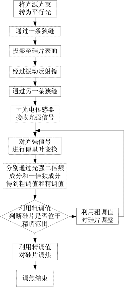
[0035] Such as figure 1 Shown, the inventive method comprises the following steps:
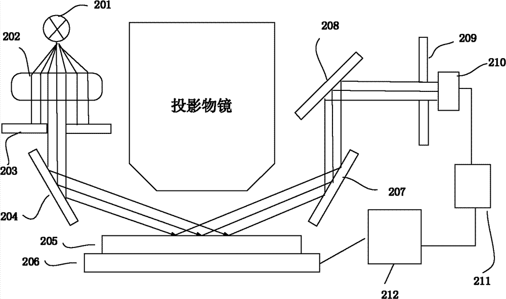
[0036] (1) Convert the light beam from the light source of the lithography machine into a parallel beam, and first project it onto the surface of the silicon wafer through a slit, and the width of the slit is recorded as d;
[0037] (2) Utilize the vibrating mirror to receive the reflected light beam on the surface of the silicon wafer, the amplitude of the vibrating mirror is 0.5d, and the frequency is denoted as f;
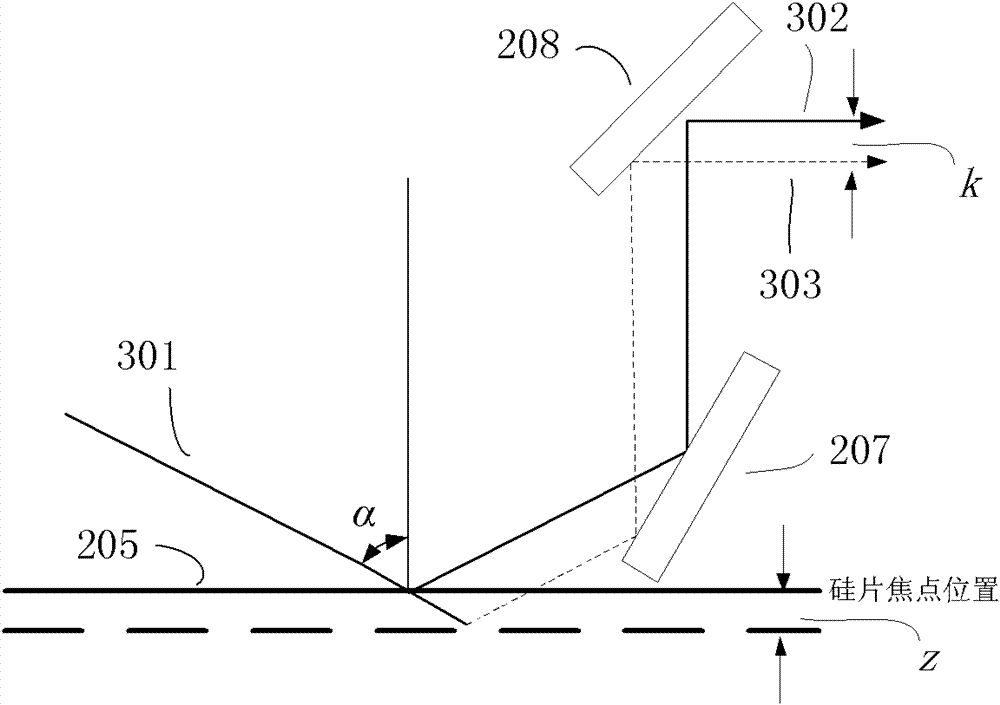
[0038] Let the defocus amount of the silicon wafer be z, and the offset of the reflected beam caused by the silicon wafer offset is recorded as k, and the relationship between the two satisfies:
[0039] k=2γ·sinα·z (I)
[0040] In the formula, γ is the magnification of the light path system from the light source to the silicon wafer, and α is the incident angle of the beam projected to the silicon wafer, both of which are constant values in the focusing system.
[0041] (3...
PUM
 Abstract
Description
Claims
Application Information