

External cavity feedback laser generation method and laser
Patent Information
- Authority / Receiving Office
- CN · China
- Current Assignee / Owner
- PEKING UNIV
- Publication Date
- 2011-02-09
- Estimated Expiration
- Not applicable · inactive patent
Smart Images
Figure 1 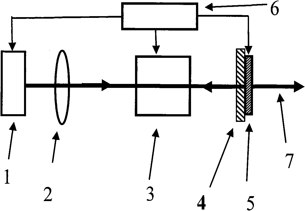
Figure 2 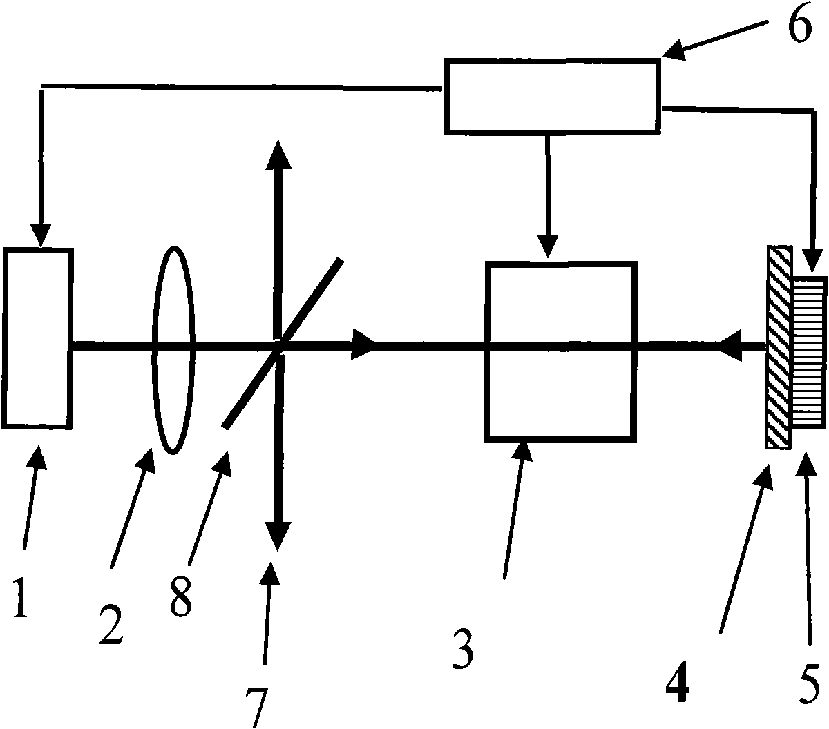
Figure 3
Abstract
Description
technical field
[0001] The invention relates to external cavity feedback laser technology, in particular to an external cavity feedback laser generation method immune to gain medium temperature and current noise and a laser, belonging to the field of laser technology. Background technique
[0002] Due to its narrow linewidth, tunable, easy frequency stabilization, small size, and compact structure, external cavity semiconductor lasers are widely used in cold atomic physics, laser spectroscopy, quantum information, metrology, environmental monitoring, and industrial measurement. . At present, semiconductor lasers of various bands in the world basically use the method of epitaxial resonator feedback (referred to as external cavity) to narrow the line width of the laser. At the same time, in order to achieve single-mode operation, there must be a mode selection element. One solution in the prior art of this kind of external cavity feedback semiconductor laser is to use a grati...