Interconnection structure, a thin film transistor substrate, and a manufacturing method thereof, as well as a display device

A technology of thin-film transistors and wiring structures, which is applied in the direction of transistors, semiconductor/solid-state device manufacturing, and electric solid-state devices. It can solve problems such as cost reduction, achieve good productivity, excellent contact resistance, and expand process margins.

Inactive Publication Date: 2011-02-09
KOBE STEEL LTD
View PDF6 Cites 6 Cited by
  • Summary
  • Abstract
  • Description
  • Claims
  • Application Information

AI Technical Summary

Problems solved by technology

For example, in order to manufacture LSI, which is a typical example of semiconductor devices, in order to prevent the occurrence of spikes (spikes) at the interface between the semiconductor layer and the Al-based alloy film, after forming a barrier metal layer such as Cr or Mo on the semiconductor layer, Al is carried out. However, in the field of semiconductor devices, process simplification and cost reduction are required

Method used


Image

  • Interconnection structure, a thin film transistor substrate, and a manufacturing method thereof, as well as a display device
  • Interconnection structure, a thin film transistor substrate, and a manufacturing method thereof, as well as a display device
  • Interconnection structure, a thin film transistor substrate, and a manufacturing method thereof, as well as a display device

Examples


no. 1 Embodiment approach

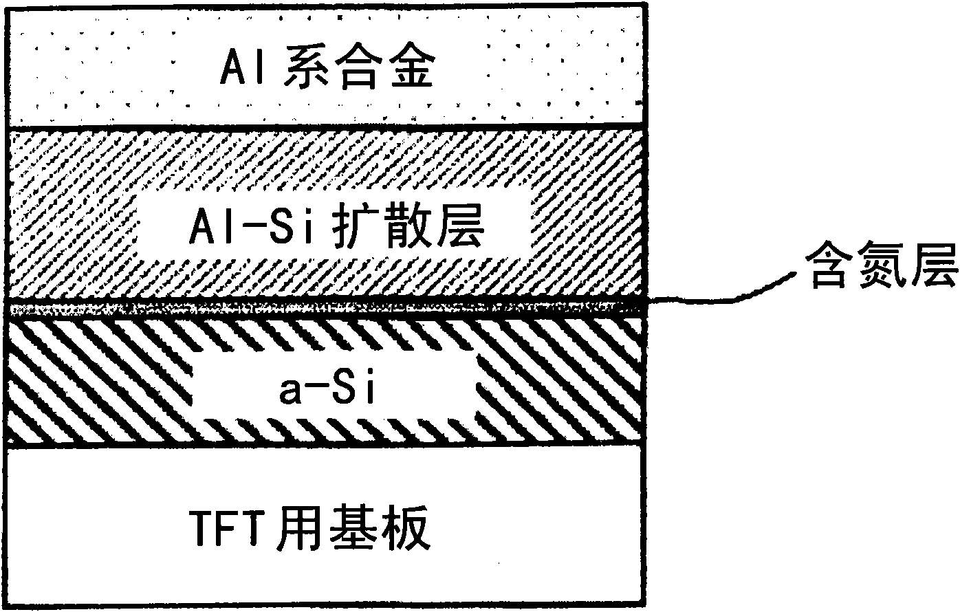
[0066] The first embodiment of the TFT of the present invention is shown in Figure 1A . exist Figure 1A Among them, there is a first semiconductor layer on the TFT substrate, a two-layer laminated structure consisting of (N, C, F) layers and an Al-Si diffusion layer is directly thereon, and a semiconductor layer is formed directly thereon. The structure of the Al alloy layer. Figure 1A The structure of can be obtained by forming the second semiconductor layer after forming the (N, C, F) layer, and then applying a heat treatment of about 150° C. or higher, for example, by the method of Example 1 described later.

[0067] In the first embodiment, the (N, C, F) layer constituting the wiring structure contains any element among nitrogen, carbon, and fluorine. Since the (N, C, F) layer is formed so as to cover almost the entire surface of the semiconductor layer, it is effective as a barrier for preventing interdiffusion of Al and Si at the interface between the Al-based alloy a...

no. 2 Embodiment approach

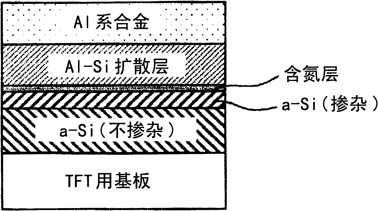
[0099] The second embodiment of the TFT of the present invention is a modified example of the Al-Si diffusion layer in the above-mentioned first embodiment, and has the following figure 2 An example of a 3-layer stack structure is shown. Specifically, since the TFT is manufactured under the condition that the interdiffusion of Al and Si does not proceed to the nitrogen-containing layer, it has a second semiconductor layer that does not substantially contain Al (that is, a semiconductor layer that is substantially only composed of Si). ), (N, C, F) layers, and an Al-Si diffusion layer in the form of a three-layer laminated structure, such a form is also included in the scope of the present invention. Here, "substantially not containing Al" means that the concentration of Al is approximately 0.01 atomic % or less when elemental analysis of Al is performed by the measuring method described later.

[0100] figure 2 The structure can be obtained, for example, by the method of E...

Embodiment approach

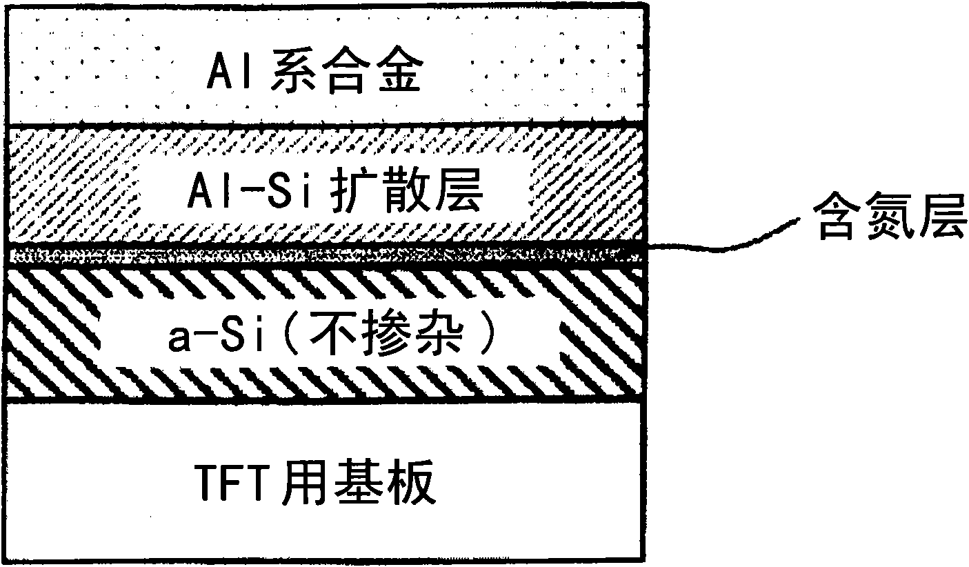
[0102] A third embodiment of the TFT of the present invention has a first semiconductor layer, a (N, C, F) layer, An example of the first semiconductor layer. In detail, it has the following structure, that is, as image 3 As shown, there are a first semiconductor layer, a (N, C, F) layer, and a first semiconductor layer on the TFT substrate, and a (N, C, F) layer and an Al-Si diffusion layer are directly placed on it. A two-layer laminated structure is formed, and an Al-based alloy layer is directly formed on top of it. image 3 The structure of can be obtained by, for example, the method of Example 3 described later. In addition, other conditions, characteristics, etc. are the same as those described in the said 1st Embodiment.

[0103] (the fourth embodiment of the present invention)

[0104] A fourth embodiment of the TFT of the present invention has a first semiconductor layer and a (N, C, F) layer between the nitrogen-containing layer and the TFT substrate constituti...


PUM

PropertyMeasurementUnit
thicknessaaaaaaaaaa
thicknessaaaaaaaaaa
thicknessaaaaaaaaaa

Abstract

Provided is a direct contact technology by which a barrier metal layer between an Al alloy wiring composed of pure Al or an Al alloy and a semiconductor layer can be eliminated and the Al alloy wiring can be directly and surely connected to the semiconductor layer within a wide process margin. In a wiring structure, the semiconductor layer, and the Al alloy film composed of the pure Al or the Al alloy are provided on the substrate in this order from the substrate side. A multilayer structure of an (N, C, F) layer containing at least one type of an element selected from among a group composed of nitrogen, carbon and fluorine, and an Al-Si diffusion layer containing Al and Si is included in this order from the substrate side, between the semiconductor layer and the Al alloy film. At least the one type of the element, i.e., nitrogen or carbon or fluorine contained in the (N, C, F) layer, is bonded with Si contained in the semiconductor layer.

Description

technical field [0001] The present invention relates to configurations of semiconductor devices applicable to flat panel displays (display devices) such as liquid crystal displays and organic EL displays, ULSI (Ultra Large Scale Integration), ASIC (Application Specific Integrated Circuit), FET (Field Effect Transistor), diodes, etc. A wire structure, a thin-film transistor substrate and a manufacturing method thereof, and a display device, particularly relating to a novel wiring structure containing pure Al or an Al-based alloy film of an Al alloy as a wiring material. Background technique [0002] Active matrix liquid crystal display devices such as liquid crystal displays are composed of thin film transistors (Thin Film Transitor, hereinafter referred to as TFT) as switching elements, transparent pixel electrodes, gate wiring, and source-drain wiring. TFT substrates such as wiring parts, amorphous silicon (a-Si) or polycrystalline silicon (p-Si) and other semiconductor lay...

Claims


Application Information

Patent Timeline
Patent Type & Authority Applications(China)
IPC IPC(8): H01L21/336H01L29/786H01L21/28H01L29/417H01L21/768H01L29/78
CPCH01L29/66575H01L21/76829H01L27/1214H01L29/458H01L21/76838H01L21/26506H01L21/2236H01L2924/0002H01L27/124H01L23/53223H01L2924/00
Inventor 川上信之越智元隆三木绫森田晋也横田嘉宏福间信也后藤裕史
Owner KOBE STEEL LTD
Why Eureka
Try Eureka