Device for controlling light-emitting diode (LED) by silicon-based MOS tube, array and manufacturing method thereof

A technology for light-emitting diodes and a manufacturing method, which is applied in the manufacturing of semiconductor/solid-state devices, semiconductor devices, instruments, etc., can solve the problems of unfavorable portable use, high power consumption, large volume, etc., and achieves improved pixels and brightness, high performance, and volume. small effect

Inactive Publication Date: 2011-02-16
FUDAN UNIV
View PDF3 Cites 8 Cited by
  • Summary
  • Abstract
  • Description
  • Claims
  • Application Information

AI Technical Summary

Problems solved by technology

At present, projectors that use separate light sources and light adjustment devices are bulky and consume a lot of power, which is not conducive to portable use

Method used


Image

  • Device for controlling light-emitting diode (LED) by silicon-based MOS tube, array and manufacturing method thereof
  • Device for controlling light-emitting diode (LED) by silicon-based MOS tube, array and manufacturing method thereof
  • Device for controlling light-emitting diode (LED) by silicon-based MOS tube, array and manufacturing method thereof

Examples


Embodiment Construction

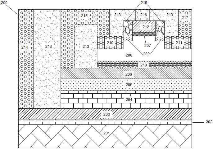
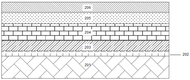
[0047] Exemplary embodiments of the present invention will be described in detail below with reference to the accompanying drawings. In the drawings, the thicknesses of layers and regions are exaggerated for convenience of illustration, and the shown sizes do not represent actual sizes. The referenced figures are schematic illustrations of idealized embodiments of the present invention, examples shown herein should not be construed as limited to the particular shapes of regions shown in the figures, but to include resulting shapes, such as manufacturing-induced deviations. For example, the curves obtained by etching are usually curved or rounded, but in the embodiment of the present invention, they are all represented by rectangles. The representation in the figure is schematic, but this should not be considered as limiting the scope of the present invention. Meanwhile, in the following description, the substrate used can be understood as including the semiconductor wafer bein...


PUM


Abstract

The invention belongs to the semiconductor device technical field, and specifically relates to a semiconductor device for controlling a light-emitting diode LED by a silicon-based MOS tube, an array and a manufacturing method thereof. The semiconductor device comprises at least two semiconductor substrates, and a silicon-based MOS transistor formed on the semiconductor substrates, and the LED. In the invention, the LED and the silicon-based MOS transistor are integrated on the same chip, thus realizing image emission only by the single chip. A plurality of the semiconductor devices can form a semiconductor device array. The projector manufactured by the method of the invention has the advantages of small volume, low power consumption, portability and the like; and by use of the integrated circuit chip, the system of the projector is greatly simplified, production cost is lowered and pixel and brightness are significantly improved.

Description

technical field [0001] The invention belongs to the technical field of semiconductor devices, and in particular relates to a semiconductor device and a manufacturing method thereof, in particular to a silicon-based MOS tube-controlled semiconductor device, an array and a manufacturing method thereof for a light-emitting diode. Background technique [0002] A projector is a projection device used to magnify and display images. At present, it has been applied to presentations in conference rooms and watching movies on a large screen by connecting DVD players and other devices at home. In movie theaters, digital cinema projectors, which have also begun to replace old film films, are used as screens for digital data on hard drives. According to different working principles, projectors can be divided into three categories: CRT, LCD, and DLP. [0003] CRT projector, also known as three-gun projector, is mainly composed of three CRT tubes. CRT (Cathode Ray Tube) is a cathode ray...

Claims


Application Information

Patent Timeline
IPC IPC(8): H01L21/8252G03B21/20H01L33/06H01L27/102
Inventor 刘昕彦王鹏飞张卫
Owner FUDAN UNIV
Why Eureka
Try Eureka