

Phosphorescent OLED having double hole-blocking layers
A technology of organic light-emitting devices and hole blocking layers, which is applied in the manufacture of semiconductor devices, electric solid devices, semiconductor/solid devices, etc., can solve problems such as efficiency loss, achieve improved hole and exciton blocking effects, and improve electron injection performance, improved external quantum efficiency, and the effects of operating life
- Summary
- Abstract
- Description
- Claims
- Application Information
AI Technical Summary
Problems solved by technology
Method used
Image

Examples
Embodiment 1~3
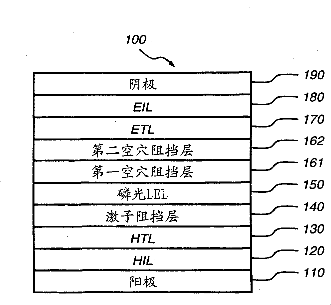
[0384] A conventional OLED (device 1) was fabricated as follows: A glass substrate of about 1.1 mm thickness coated with a transparent ITO conductive layer was cleaned using a commercially available glass washer tool and dried. The thickness of ITO is about 22 nm, and the sheet resistance of ITO is about 68Ω / square. The surface of the ITO is then treated with an oxidizing plasma to render the surface suitable for use as an anode. By decomposing CHF in an RF plasma treatment chamber 3 Gas deposits a layer of CF on the clean ITO surface x (1nm thick) as the anode buffer layer. The substrate is then transferred to a vacuum deposition chamber to deposit all other layers on top of the substrate. by about 10 -6 The following layers were deposited in the following order by evaporating from a heated boat under a vacuum of Torr:
[0385] a) HTL, 100 nm thick, containing N,N'-di-1-naphthyl-N,N'-diphenyl-4,4'-diaminobiphenyl (NPB);
[0386] b) EXBL, 10 nm thick, containing 4-(9H-ca...
Embodiment 4~5
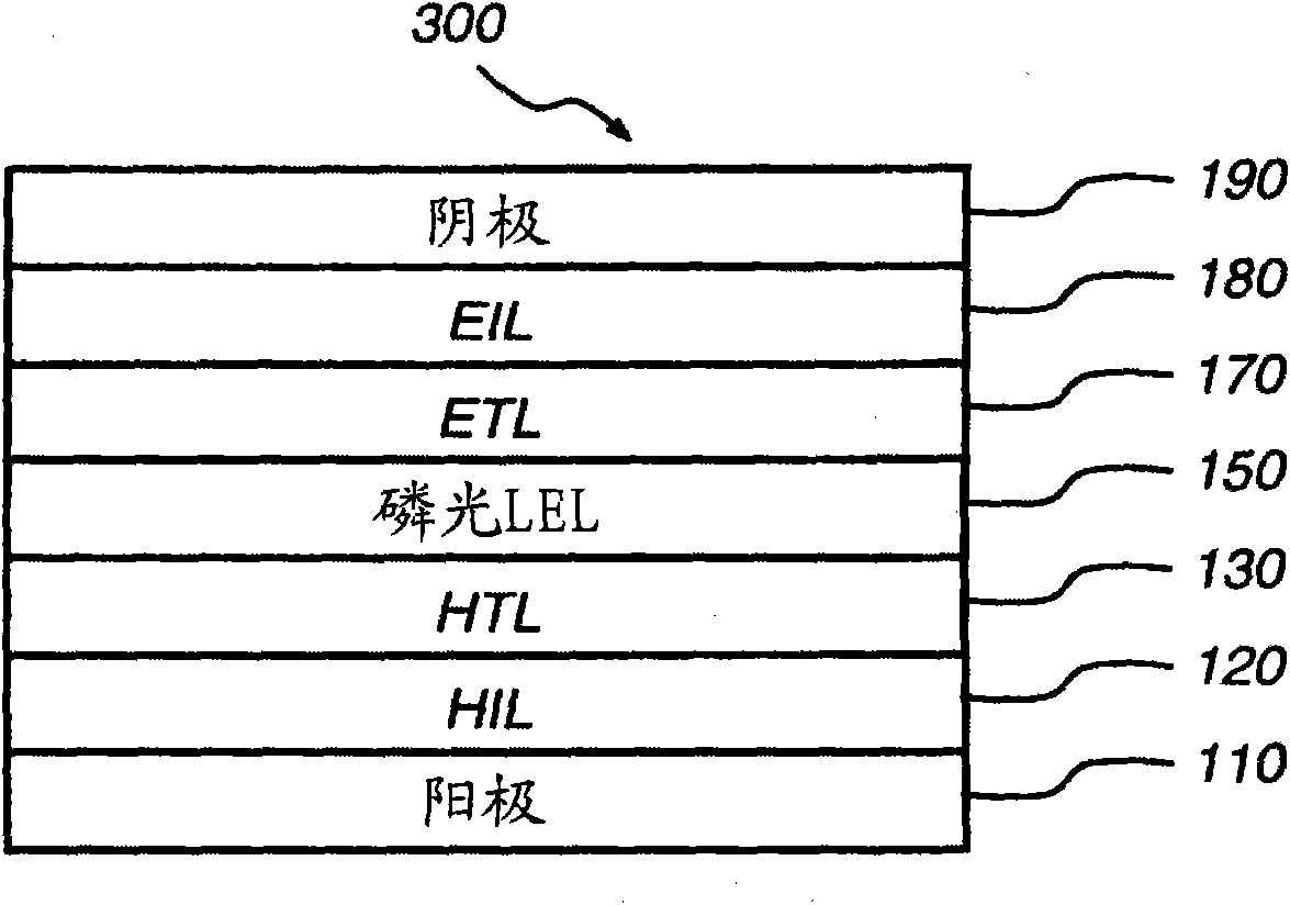
[0416] A comparative phosphorescent OLED (device 4) was produced in the same manner as in Example 1 with the same layer structure.
[0417] Device 4 is shown below: ITO / 100nm NPB / 10nm TCTA / 20nm CBP: 6% Ir(ppy) 3 / 25nm Bphen / 15nm Bphen: 1.0% Li / 100nm Al. The EL performance of the device is summarized in Table 1.
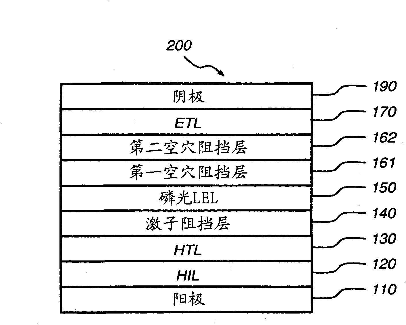
[0418] A phosphorescent OLED (device 5) of the present invention was fabricated in the same manner as in Example 4 with the same layer structure, except that there were 2 HBLs in the device. The layer structure is as follows:
[0419] a) HTL, 100 nm thick, containing NPB;
[0420] b) EXBL, 10 nm thick, containing TCTA;
[0421] c) LEL, 20nm thick, containing Ir(ppy) doped with 6% by volume 3 CBP;
[0422] d) The first HBL, 5nm thick, contains formula (X-1) (HOMO energy<-6.1eV, LUMO energy=-2.73eV, triplet energy=2.95eV);
[0423] e) a second HBL, 20 nm thick, comprising Bphen;
[0424] f) ETL, 15 nm thick, comprising Bphen doped with about 1.0% lithium; and
...
Embodiment 6~8
[0432] A comparative phosphorescent OLED (device 6) was produced in the same manner as in Example 1 with the same layer structure. The layer structure is as follows:
[0433] a) HIL, 10 nm thick, comprising hexaazatriphenylene hexanitrile (HAT-CN);
[0434] b) HTL, 120nm thick, containing NPB;
[0435] c) EXBL, 10 nm thick, containing TCTA;
[0436] d) LEL, 20nm thick, containing Ir(piq) doped with 4% by volume 3 The formula (OP-1) (HOMO energy=-5.97eV, LUMO energy=-2.66eV, triplet energy=2.18eV);
[0437] e) a first ETL, 20nm thick, comprising formula (OP-1);
[0438] f) a second ETL, 35 nm thick, comprising Bphen doped with about 1.0 vol% lithium; and
[0439] g) Cathode: about 100 nm thick, containing Al.
[0440] Device 6 is shown below: ITO / 10nm HAT-CN / 120nm NPB / 10nm TCTA / 20nm(OP-1): 4% Ir(piq) 3 / 20nm(OP-1) / 35nm Bphen: 1.0% Li / 100nm Al. The EL performance of the device is summarized in Table 2. The device does not have any HBL because the first ETL is formed from...
PUM
 Abstract
Description
Claims
Application Information