Supercharge Your Innovation With Domain-Expert AI Agents!

Method for manufacturing source-drain region

A manufacturing method and technology of source and drain regions, applied in semiconductor/solid-state device manufacturing, electrical components, circuits, etc., can solve problems such as difficult control, high sensitivity of device temperature, easy diffusion of impurities, etc., to achieve sensitivity reduction, easy to control effects

Inactive Publication Date: 2011-03-30
SEMICON MFG INT (SHANGHAI) CORP
View PDF0 Cites 0 Cited by
  • Summary
  • Abstract
  • Description
  • Claims
  • Application Information

AI Technical Summary

Problems solved by technology

This will bring about a problem: as the junction depth becomes shallower, the impurity concentration gradient will become larger and larger, and then the impurities will easily diffuse during subsequent thermal processes such as annealing; that is to say, the junction depth becomes Shallow will make the device more and more sensitive to temperature, making it difficult to control as required

Method used


Image

  • Method for manufacturing source-drain region
  • Method for manufacturing source-drain region
  • Method for manufacturing source-drain region

Examples


Embodiment Construction

[0032] Aiming at the problems existing in the prior art, the present invention proposes an improved method for manufacturing source and drain regions. When performing LDD implantation, it uses higher energy than the existing LDD process or lower impurity dose than the existing LDD process. Preferably, higher energy and lower impurity dose than the existing LDD process can also be used at the same time.

[0033] In order to make the object, technical solution, and advantages of the present invention clearer, the solutions of the present invention will be further described in detail below with reference to the accompanying drawings and examples.

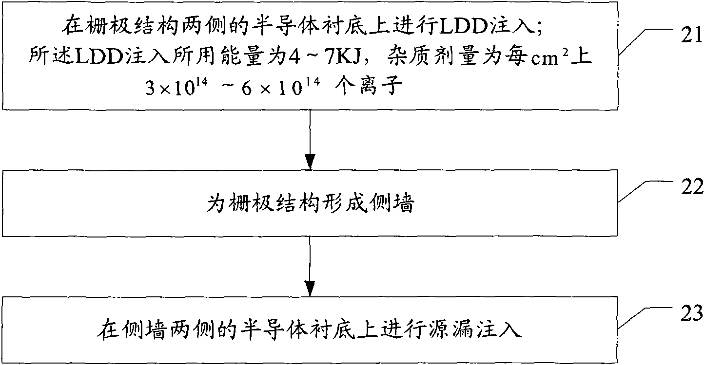
[0034] figure 1 It is a flow chart of an embodiment of the method for manufacturing the source and drain regions of the present invention. It is assumed that in this embodiment, the energy and impurity dose of the LDD implantation are changed at the same time. Such as figure 1 shown, including the following steps:

[0035] Step 21:...


PUM


Abstract

The invention discloses a method for manufacturing a source-drain region. The method comprises the following steps of: carrying out LDD (Lightly Doped Drain) injection on semiconductor substrates at both sides of a grid structure, wherein the LDD injection consumes the energy of 4-7 kJ or the impurity dosage is 3*1014-6*1014 atoms per square centimeter or the consumed energy is 4-7 kJ while the impurity dosage is 3*1014-6*1014 atoms per square centimeter; and forming a side wall for the grid structure and carrying out source-drain injection on the semiconductor substrates at both sides of the side wall. The method for manufacturing the source-drain region of the invention can be used to lower the temperature sensitivity of a device and improve the high threshold voltage performance of the device.

Description

technical field [0001] The invention relates to the technical field of manufacturing semiconductor components, in particular to a method for manufacturing source and drain regions. Background technique [0002] In the existing complementary metal oxide semiconductor (CMOS) and other technologies, after forming the N well and the P well, and completing the fabrication of shallow trench isolation and gate structure, it is necessary to manufacture the source and drain regions. [0003] The manufacturing process of the existing source and drain regions mainly includes the following steps: [0004] Step 11: Perform lightly doped drain (LDD) implantation on the semiconductor substrate on both sides of the gate structure. [0005] As the width of the gate structure decreases, the length of the channel below it also decreases, and the decrease in the channel length increases the possibility of charge penetration between the source and drain, that is, an undesirable leakage current ...

Claims


Application Information

Patent Timeline
Patent Type & Authority Applications(China)
IPC IPC(8): H01L21/336H01L21/265H01L21/8238
Inventor 刘兵武居建华
Owner SEMICON MFG INT (SHANGHAI) CORP
Features
  • R&D
  • Intellectual Property
  • Life Sciences
  • Materials
  • Tech Scout
  • Unparalleled Data Quality
  • Higher Quality Content
  • 60% Fewer Hallucinations
Learn More